Supercharge Your Innovation With Domain-Expert AI Agents!

Method of manufacturing semiconductor apparatus

a manufacturing method and semiconductor technology, applied in the direction of electrical equipment, semiconductor devices, basic electric elements, etc., can solve the problems of miniaturization limit and cost increas

Active Publication Date: 2020-09-01
OKAMOTO MACHINE TOOL WORKS LTD
View PDF2 Cites 0 Cited by
  • Summary
  • Abstract
  • Description
  • Claims
  • Application Information

AI Technical Summary

Problems solved by technology

However, limitations on miniaturization, and cost increase have become problems.

Method used


Image

  • Method of manufacturing semiconductor apparatus
  • Method of manufacturing semiconductor apparatus
  • Method of manufacturing semiconductor apparatus

Examples


Embodiment Construction

[0015]In the following detailed description, for purpose of explanation, numerous specific details are set forth in order to provide a thorough understanding of the disclosed embodiments. It will be apparent, however, that one or more embodiments may be practiced without these specific details. In other instances, well-known structures and devices are schematically shown in order to simplify the drawing.

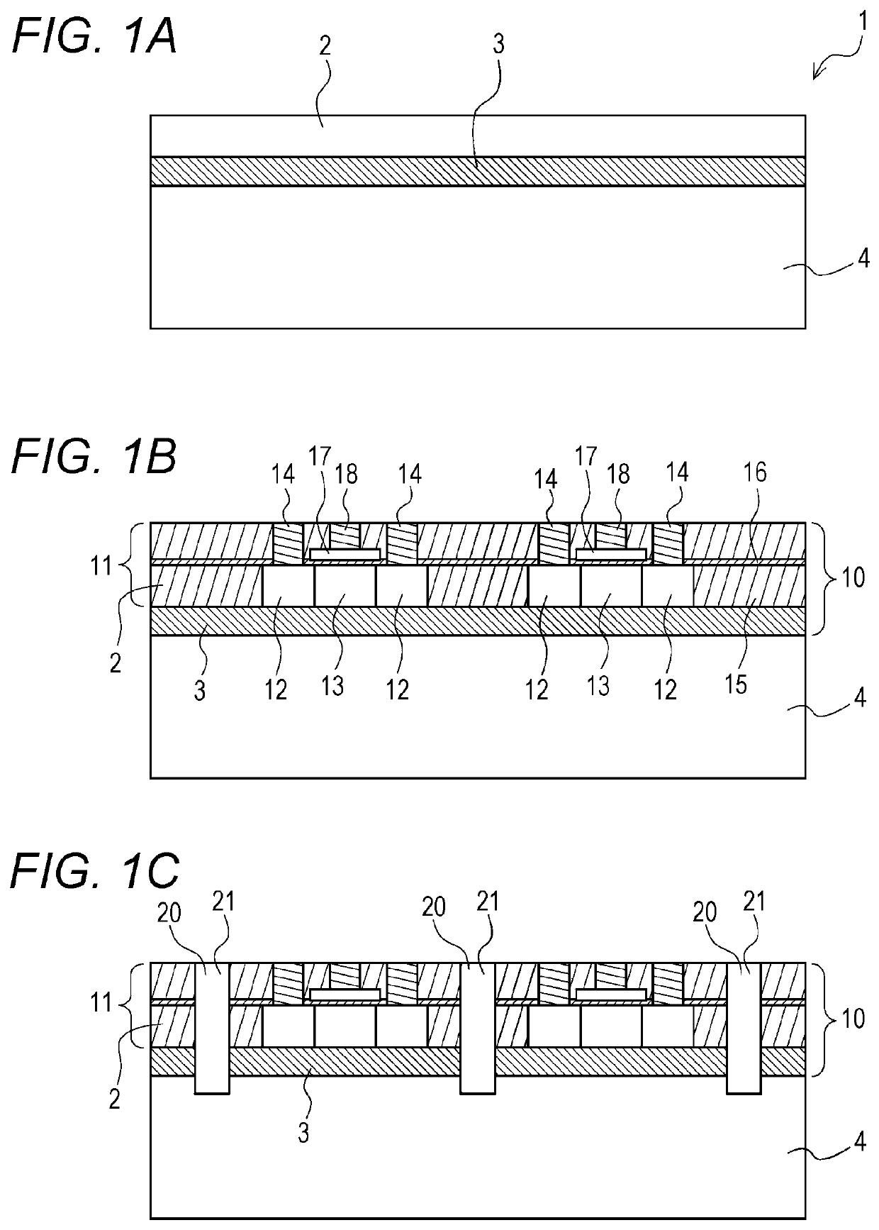
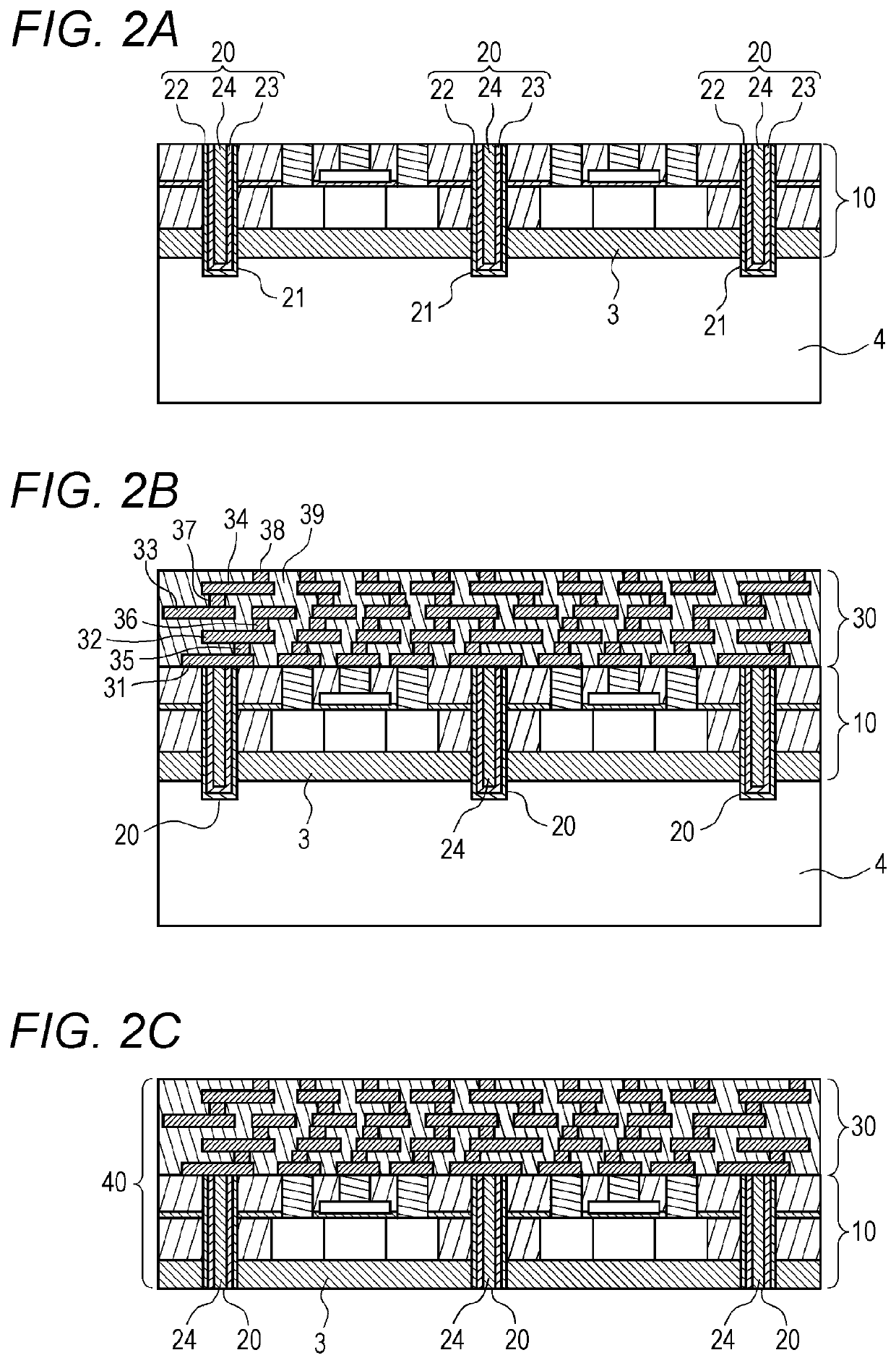
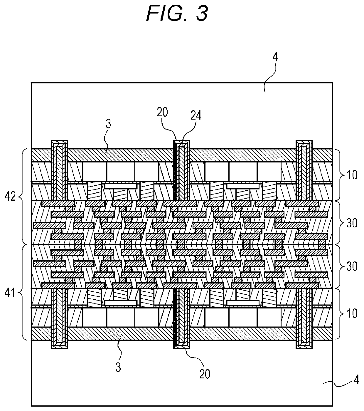
[0016]In the field of semiconductor apparatuses, in order to realize more three-dimensional multilayered devices (three-dimensional devices), it is necessary to further reduce a thickness of each device wafer, improve inter-device connection stability (yield), and reduce costs. Currently there are many process and structural challenges. Therefore, development is underway both domestically and overseas.

[0017]Specifically, a semiconductor device wafer currently has a thickness of 30 to 40 μm. In the future, the semiconductor device wafer is required to have ultra-thin layers of 5 to 20...


PUM

PropertyMeasurementUnit
thicknessaaaaaaaaaa
thicknessaaaaaaaaaa
thicknessaaaaaaaaaa

Abstract

An embodiment of the present disclosure provides a method of manufacturing a semiconductor apparatus, including the following steps. A) forming a semiconductor device element in a Si active layer of an insulating isolation Si substrate including the Si active layer, a buried insulating layer, and a Si supporting substrate arranged in this order; B) forming a plurality of through electrode holes penetrating the Si active layer and the buried insulating layer to reach a partial region of the Si supporting substrate in an element region layer including the formed semiconductor device element; C) forming a through silicon via by sequentially forming an insulating film, a barrier film, and a Cu film inside the through electrode hole to completely fill the through electrode hole; D) forming a multilayer wiring layer including a wiring layer connected to the semiconductor device element on an outer surface of the element region layer in which the through silicon via is formed; and E) exposing the Cu film of the through silicon via by removing the Si supporting substrate after forming the multilayer wiring layer.

Description

CROSS-REFERENCE TO RELATED APPLICATION[0001]This application claims priority from Japanese Patent Application No. 2018-019791 filed with the Japan Patent Office on Feb. 7, 2018, the entire content of which is hereby incorporated by reference.BACKGROUND1. Technical Field[0002]The present disclosure relates to a method of manufacturing a semiconductor apparatus.2. Related Art[0003]For a semiconductor device, it is required to transmit more information more quickly and to be compact and have low power consumption. Conventionally, these requirements and the like have been solved by a technique of miniaturizing the semiconductor device.[0004]However, limitations on miniaturization, and cost increase have become problems. Therefore, as an alternative to miniaturization, the semiconductor device is being three-dimensionally formed by through silicon via (TSV).[0005]For example, JP-A-2015-023113 discloses a method for flattening and grinding a semiconductor substrate with a copper through e...

Claims


Application Information

Patent Timeline
Patent Type & Authority Patents(United States)
IPC IPC(8): H01L21/768H01L21/762H01L25/00H01L25/065
CPCH01L21/76898H01L21/76831H01L21/76877H01L21/7624H01L21/76243H01L25/50H01L25/0657H01L2225/06524H01L2225/06527H01L2225/06541H01L21/76846H01L21/7685H01L21/76865H01L21/28506H01L21/304
Inventor YAMAMOTO, EIICHIMITSUI, TAKAHIKO
Owner OKAMOTO MACHINE TOOL WORKS LTD
Features
  • R&D
  • Intellectual Property
  • Life Sciences
  • Materials
  • Tech Scout
  • Unparalleled Data Quality
  • Higher Quality Content
  • 60% Fewer Hallucinations
Learn More