AI technical title is built by Patsnap AI team. It summarizes the technical point description of the patent document.
a quantum detector and multi-stage technology, applied in the field of quantum computing, can solve the problems of tens of milli-kelvin (mk) temperatures, large superconducting structure, noisy current physical quantum computers, etc., and achieve the effect of reducing the loading of the quantum structure, enhancing the rejection of environmental parasitic electric and/or magnetic fields, and eliminating the loading
Active Publication Date: 2020-11-24
EQUAL1 LABS INC
View PDF53 Cites 4 Cited by
Summary
Abstract
Description
Claims
Application Information
AI Technical Summary
This helps you quickly interpret patents by identifying the three key elements:
Problems solved by technology
Method used
Benefits of technology
Benefits of technology
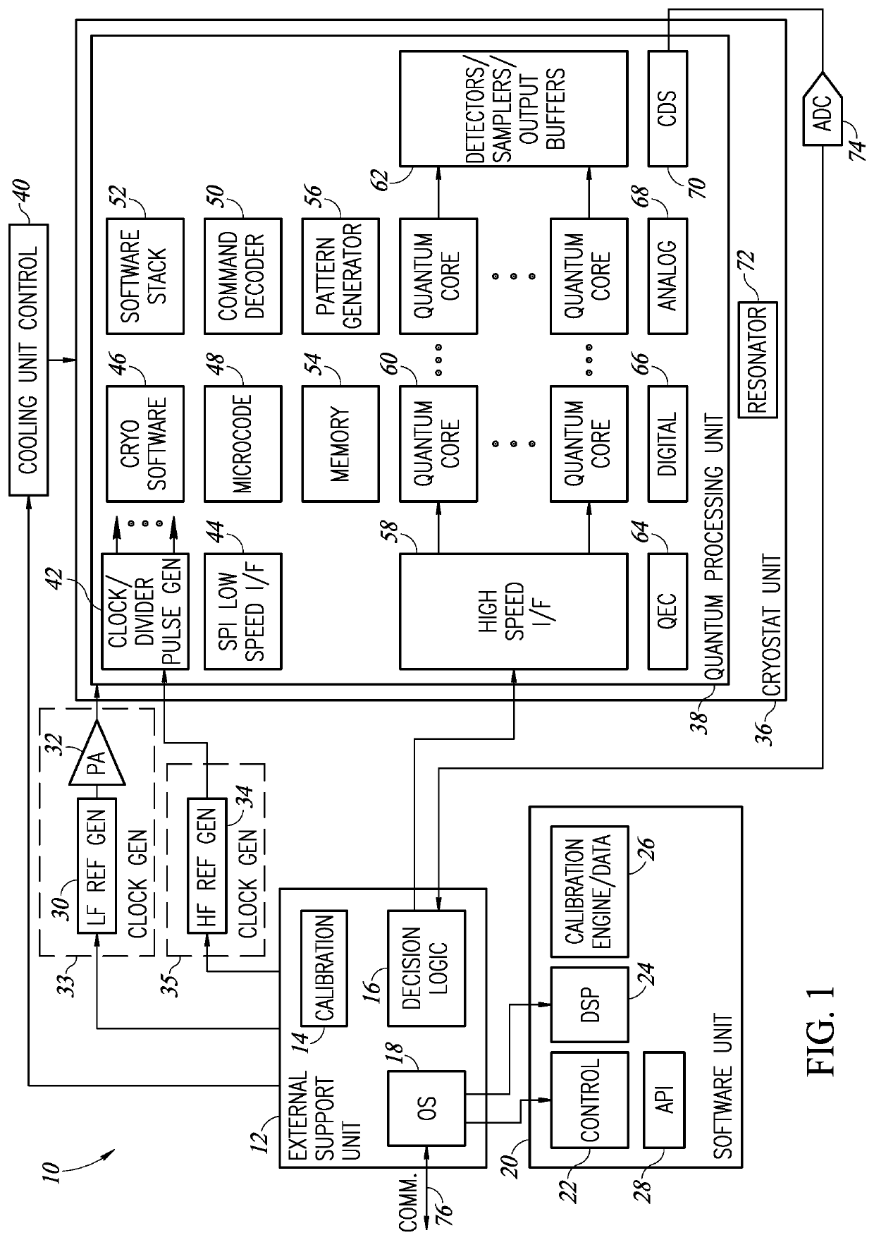
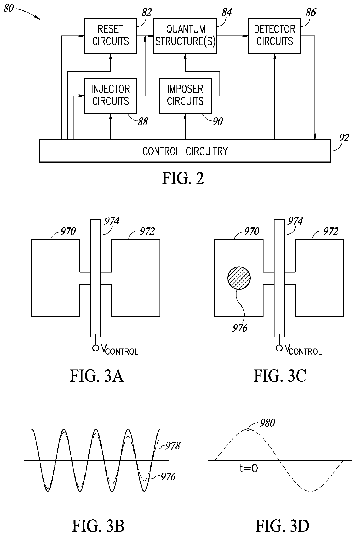
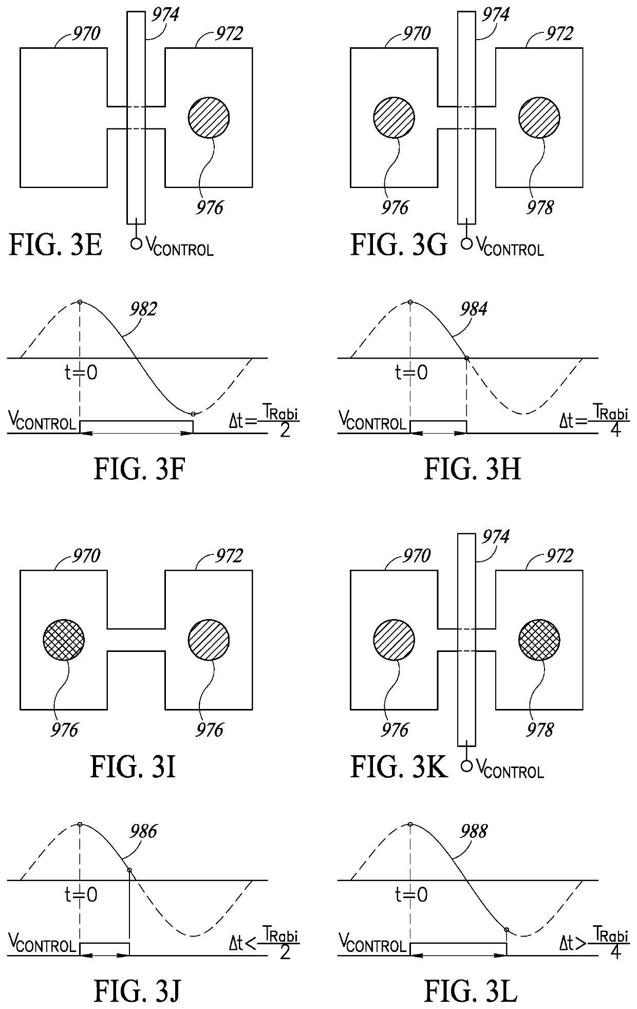
[0009]The present invention is a multistage semiconductor quantum detector circuit incorporating an anticorrelation mechanism. The quantum structure has at least the first stage sensor of the detector merged into the quantum structure in order to minimize loading of the quantum structure. The merged quantum structure and detector sensor may be encapsulated in a metal cage in order to provide enhanced rejection of the environmental parasitic electric and / or magnetic fields. A double boot strapping detector front-end configuration substantially eliminates the loading coming from both the gate-source and the gate-drain parasitic capacitances of the first sensor device of the detector that is connected to the quantum structure. In addition, differential detection aids in rejecting leakage, noise, and correlated interference coupling. Both dummy referenced differential detection as well as self-referenced differential detection may be employed in the detector. Moreover, correlated double sampling is used after preamplification in the detector in order to further reject noise and perturbations in the system.
Problems solved by technology
The key challenge of quantum computing is isolating such microscopic particles, loading them with the desired information, letting them interact and then preserving the result of their quantum interaction.
Current physical quantum computers, however, are very noisy and quantum error correction is commonly applied to compensate for the noise.
Their main drawbacks, however, are the fact that superconducting structures are very large and costly and have difficulty in scaling to quantum processor sizes of thousands or millions of quantum-bits (qubits).
Furthermore, they need to operate at few tens of milli-kelvin (mK) temperatures, that are difficult to achieve and where it is difficult to dissipate significant power to operate the quantum machine.
Method used
Image
Click on the blue label to locate the original text in one second.
Reading with bidirectional positioning of images and text.
Examples
Embodiment Construction
[0226]In the following detailed description, numerous specific details are set forth in order to provide a thorough understanding of the invention. It will be understood by those skilled in the art, however, that the present invention may be practiced without these specific details. In other instances, well-known methods, procedures, and components have not been described in detail so as not to obscure the present invention.
[0227]Among those benefits and improvements that have been disclosed, other objects and advantages of this invention will become apparent from the following description taken in conjunction with the accompanying figures. Detailed embodiments of the present invention are disclosed herein; however, it is to be understood that the disclosed embodiments are merely illustrative of the invention that may be embodied in various forms. In addition, each of the examples given in connection with the various embodiments of the invention which are intended to be illustrative...
PUM
Abstract
A novel and useful multistage semiconductor quantum detector circuit incorporating an anticorrelation mechanism. The quantum structure has at least the first stage sensor of the detector merged into the quantum structure in order to minimize loading of the quantum structure. The merged quantum structure and detector sensor may be encapsulated in a metal cage in order to provide enhanced rejection of the environmental parasitic electric and / or magnetic fields. A double boot strapping detector front-end configuration substantially eliminates the loading coming from both the gate-source and the gate-drain parasitic capacitances of the first sensor device of the detector that is connected to the quantum structure. In addition, differential detection aids in rejecting leakage, noise, and correlated interference coupling. Both dummy referenced differential detection as well as self-referenced differential detection may be employed in the detector. Moreover, correlated double sampling is used after preamplification in the detector in order to further reject noise and perturbations in the system.
Description
REFERENCE TO PRIORITY APPLICATIONS[0001]This application is a continuation-in-part of U.S. application Ser. No. 16 / 445,645, filed Jun. 19, 2019, entitled “Semiconductor Controlled Quantum Interaction Gates,” which claims the benefit of U.S. Provisional Application No. 62 / 687,800, filed Jun. 20, 2018, entitled “Electric Signal Pulse-Width And Amplitude Controlled And Re-Programmable Semiconductor Quantum Rotation Gates,” U.S. Provisional Application No. 62 / 687,803, filed Jun. 21, 2018, entitled “Semiconductor Quantum Structures and Computing Circuits Using Local Depleted Well Tunneling,” U.S. Provisional Application No. 62 / 689,100, filed Jun. 23, 2018, entitled “Semiconductor Controlled Entangled-Aperture-Logic Quantum Shift Register,” U.S. Provisional Application No. 62 / 694,022, filed Jul. 5, 2018, entitled “Double-V Semiconductor Entangled-Aperture-Logic Parallel Quantum Interaction Path,” U.S. Provisional Application No. 62 / 687,779, filed Jun. 20, 2018, entitled “Semiconductor Qua...
Claims
Application Information
Patent Timeline
Application Date:The date an application was filed.
Publication Date:The date a patent or application was officially published.
First Publication Date:The earliest publication date of a patent with the same application number.
Issue Date:Publication date of the patent grant document.
PCT Entry Date:The Entry date of PCT National Phase.
Estimated Expiry Date:The statutory expiry date of a patent right according to the Patent Law, and it is the longest term of protection that the patent right can achieve without the termination of the patent right due to other reasons(Term extension factor has been taken into account ).
Invalid Date:Actual expiry date is based on effective date or publication date of legal transaction data of invalid patent.

