Method of writing data in nonvolatile memory device, with divided subpages or subblocks, and method of erasing data in nonvolatile memory device with divided subpages or subblocks

a nonvolatile memory device and data technology, applied in static storage, digital storage, instruments, etc., can solve the problem of power-off loss of content stored therein, and achieve the effect of efficient writing data

Active Publication Date: 2021-01-19
SAMSUNG ELECTRONICS CO LTD
View PDF35 Cites 2 Cited by
  • Summary
  • Abstract
  • Description
  • Claims
  • Application Information

AI Technical Summary

Benefits of technology

[0004]At least one example embodiment of the present disclosure provides a method of efficiently writing data in a nonvolatile memory device that includes memory cells stacked in three dimensions.
[0005]At least one example embodiment of the present disclosure provides a method of efficiently erasing data in a nonvolatile memory device that includes memory cells stacked in three dimensions.

Problems solved by technology

Volatile memory devices may perform read and write operations at a high speed, while contents stored therein may be lost at power-off.

Method used


Image

  • Method of writing data in nonvolatile memory device, with divided subpages or subblocks, and method of erasing data in nonvolatile memory device with divided subpages or subblocks
  • Method of writing data in nonvolatile memory device, with divided subpages or subblocks, and method of erasing data in nonvolatile memory device with divided subpages or subblocks
  • Method of writing data in nonvolatile memory device, with divided subpages or subblocks, and method of erasing data in nonvolatile memory device with divided subpages or subblocks

Examples


Embodiment Construction

[0025]Various example embodiments will be described more fully with reference to the accompanying drawings, in which embodiments are shown. The present disclosure may, however, be embodied in many different forms and should not be construed as limited to the embodiments set forth herein. Like reference numerals refer to like elements throughout this application.

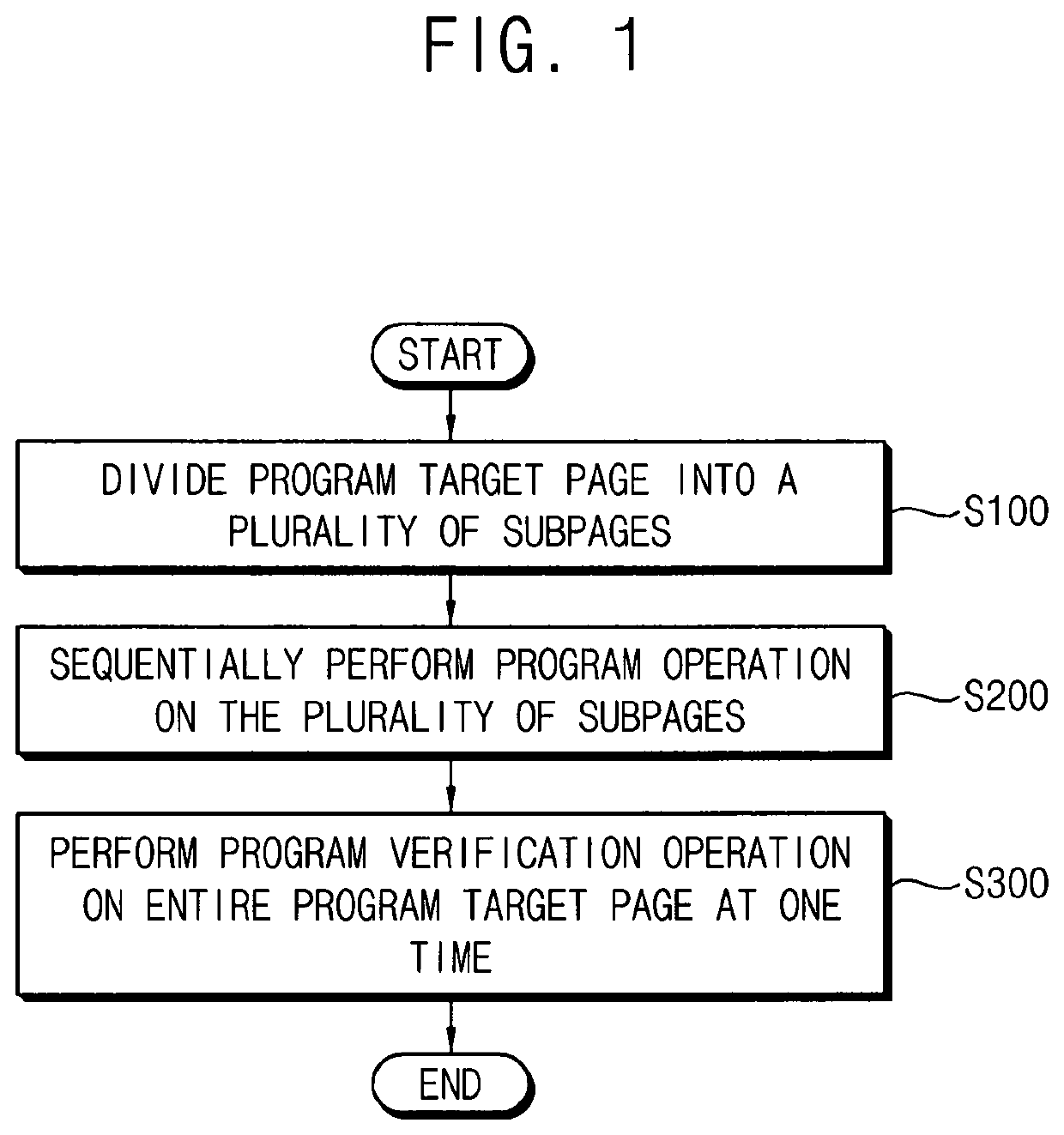
[0026]FIG. 1 is a flow chart illustrating a method of writing data in a nonvolatile memory device according to example embodiments.

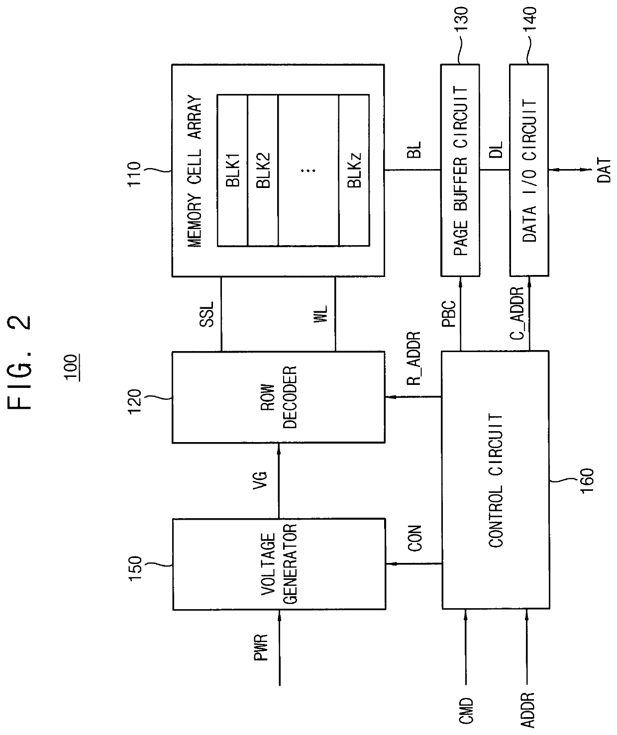
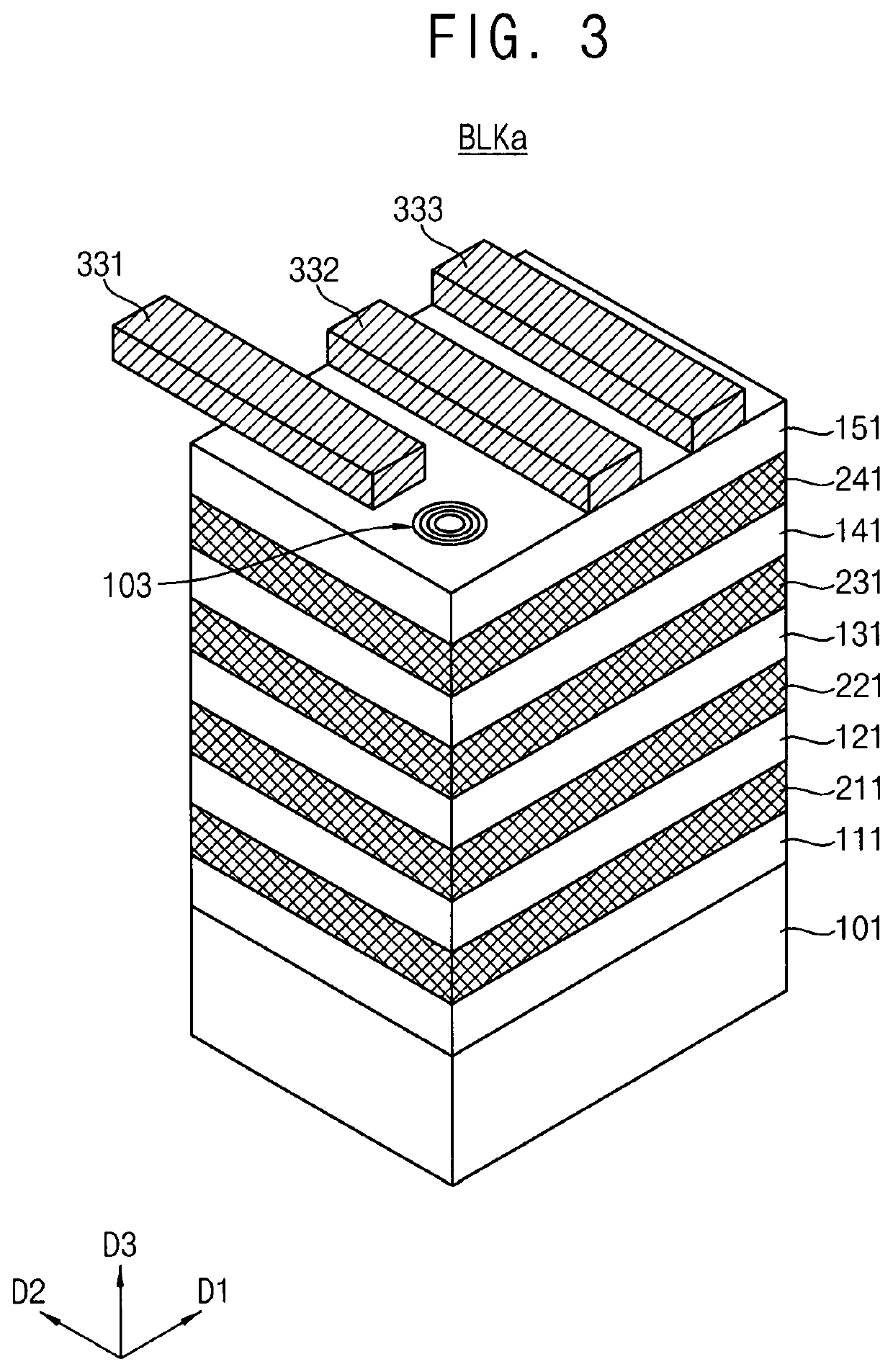
[0027]Referring to FIG. 1, a method of writing data according to example embodiments is performed by a nonvolatile memory device including a plurality of cell strings, and each of the plurality of cell strings includes a plurality of memory cells disposed in a vertical direction. For example, each cell string includes a plurality of memory cells that are stacked in a direction intersecting (e.g., substantially perpendicular to) a substrate. Configurations of the nonvolatile memory device will be d...


PUM


Abstract

In a method of writing data in a nonvolatile memory device including a plurality of cell strings, each of the plurality of cell strings includes a plurality of memory cells disposed in a vertical direction. A program target page is divided into a plurality of subpages. The program target page is connected to one of a plurality of wordlines. Each of the plurality of subpages includes memory cells that are physically spaced apart from one another. A program operation is sequentially performed on the plurality of subpages. A program verification operation is performed on the program target page including the plurality of subpages at a time.

Description

CROSS-REFERENCE TO RELATED APPLICATION[0001]This application claims the benefit of priority under 35 U.S.C. § 119 to Korean Patent Application No. 10-2018-0080398, filed Jul. 11, 2018, in the Korean Intellectual Property Office (KIPO), the contents of which are herein incorporated by reference in their entirety.BACKGROUND1. Technical Field[0002]Example embodiments relate generally to semiconductor memory devices, and more particularly to methods of writing data in nonvolatile memory devices, methods of erasing data in nonvolatile memory devices, and nonvolatile memory devices performing the methods.2. Description of the Related Art[0003]Semiconductor memory devices can generally be divided into two categories, depending upon whether or not they retain stored data when disconnected from a power supply. These categories include volatile memory devices, which lose stored data when disconnected from power, and nonvolatile memory devices, which retain stored data when disconnected from p...

Claims


Application Information

Patent Timeline
Patent Type & Authority Patents(United States)
IPC IPC(8): G11C13/00G11C7/12G11C16/34G11C16/10G11C16/14G11C11/56
CPCG11C13/0069G11C7/12G11C11/5628G11C11/5642G11C13/0026G11C16/10G11C16/14G11C16/3436G11C16/3454G11C16/3459G11C13/0064G11C13/0097G11C2013/0085G11C11/5678G11C13/0004G11C13/0028G11C13/003G11C2213/71G11C2213/79G11C5/025H10B63/845H10N70/823H10N70/231H10N70/8822H10N70/8825H10N70/8836H10N70/884H10N70/8828H10N70/8833G11C16/30G11C16/3445H10B41/27H10B43/27
Inventor KANAMORI, KOHJIKANG, CHANG-SEOKKIM, YONG-SEOKLEE, KYUNG-HWAN
Owner SAMSUNG ELECTRONICS CO LTD
Why Eureka
Try Eureka