Nano-scale LED element for horizontally-aligned assembly, method for manufacturing same, and horizontally-aligned assembly comprising same micro-LED

a technology of led elements and horizontal alignment, which is applied in the direction of nanostructure manufacturing, lighting and heating apparatus, and nanostructure assembly, etc., can solve the problems of difficult placement and mounting of nano-scale led elements on electrodes, nano- or micro-scale devices, and inability to individually arrange and mount nano-scale led elements in target electrode regions. , to achieve the effect of improving the alignment of led elements, improving the number of led elements, and easy assembly

Active Publication Date: 2021-02-02
SAMSUNG DISPLAY CO LTD
View PDF53 Cites 7 Cited by
  • Summary
  • Abstract
  • Description
  • Claims
  • Application Information

AI Technical Summary

Benefits of technology

[0010]A first objective of the present invention is to provide a nano-scale light-emitting diode (LED) element for a horizontal array assembly that can be easily laid in a length direction and mounted on a desired electrode region, and a manufacturing method thereof. According to the present invention, it is possible to improve an alignment of LED elements mounted on a desired electrode region to significantly increase the number of LED elements that are included per unit area of an electrode line and significantly improve electrical connectivity between the electrode and the LED elements.
[0011]A second objective of the present invention is to provide a horizontal array assembly that can significantly increase the number of nano-scale LED elements that are mounted per unit area of an electrode line by utilizing the nano-scale LED element according to the present invention, and that can have a good electrical connectivity between an electrode and the nano-scale LED elements to emit light without faults and achieve a desired quantity of light when power is applied to the electrode.
[0034]The present invention can implement a nano-scale light-emitting diode (LED) element that can be easily laid in a length direction and mounted on a desired electrode region to improve an alignment of the mounted element. As a result, it is possible to significantly increase the number of LED elements that are included per unit area of an electrode line and significantly improve electrical connectivity between the electrode and the LED elements. The present invention can also implement a horizontal array assembly that can significantly increase the number of nano-scale LED elements that are mounted per unit area of an electrode line, achieve a desired quantity of light by emitting light without faults when power is applied thereto due to good electrical connectivity between the electrode and the mounted nano-scale LED elements, increase a usage lifetime thereof due to an increase in durability of the LED elements along and a decrease in heat generation, and increase luminous efficiency due to an increase in the number of elements. Accordingly, the present invention is applicable to various fields such as lights, displays, etc.

Problems solved by technology

In particular, methods of mounting nano-scale LED elements on electrodes still have difficulties in that it is very difficult to place and mount nano-scale LED elements on electrodes as intended because of a limitation of a size of each of the nano-scale LED elements.
This is because nano-scale LED elements are nano- or micro-scale devices and cannot be individually arranged and mounted in a target electrode region with human hands.
In addition, it is very difficult to control the number of nano-scale LED elements included in a unit electrode region, a positional relationship between an electrode and the nano-scale LED elements, etc. when the nano-scale LED elements are mounted in a target electrode region, and it is also difficult to obtain a high quantity of light due to a limitation in the number of LED elements included in a unit area when the LED elements are arranged in a two-dimensional plane.
Furthermore, it is further difficult to obtain a desired quantity of light because not all nano-scale LED elements connected to two different electrodes can emit light without a defect such as an electrical short.

Method used


Image

  • Nano-scale LED element for horizontally-aligned assembly, method for manufacturing same, and horizontally-aligned assembly comprising same micro-LED
  • Nano-scale LED element for horizontally-aligned assembly, method for manufacturing same, and horizontally-aligned assembly comprising same micro-LED
  • Nano-scale LED element for horizontally-aligned assembly, method for manufacturing same, and horizontally-aligned assembly comprising same micro-LED

Examples


Embodiment Construction

[0052]Hereinafter, preferred embodiments of the present invention will be described in detail with reference to the accompanying drawings.

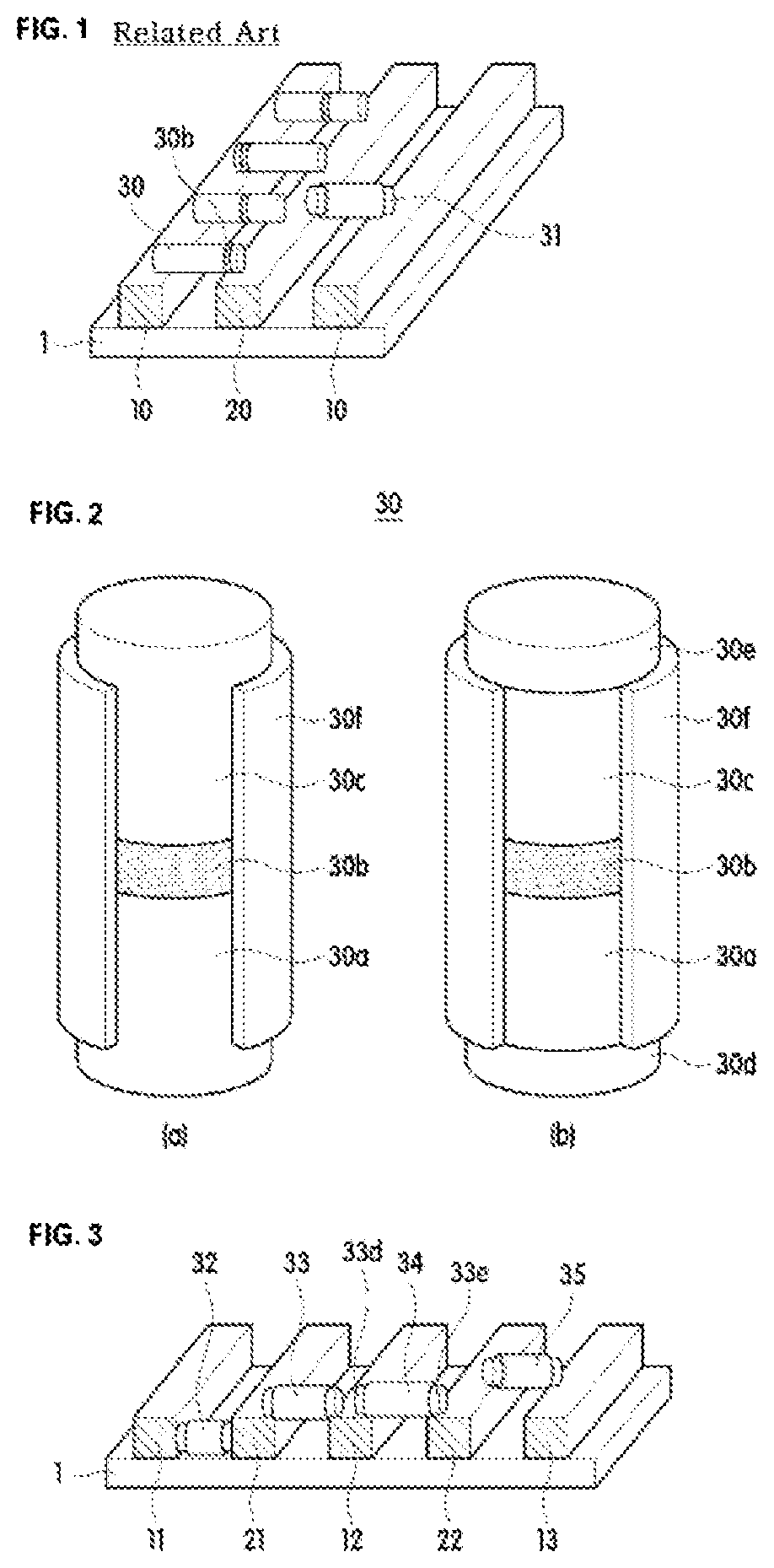
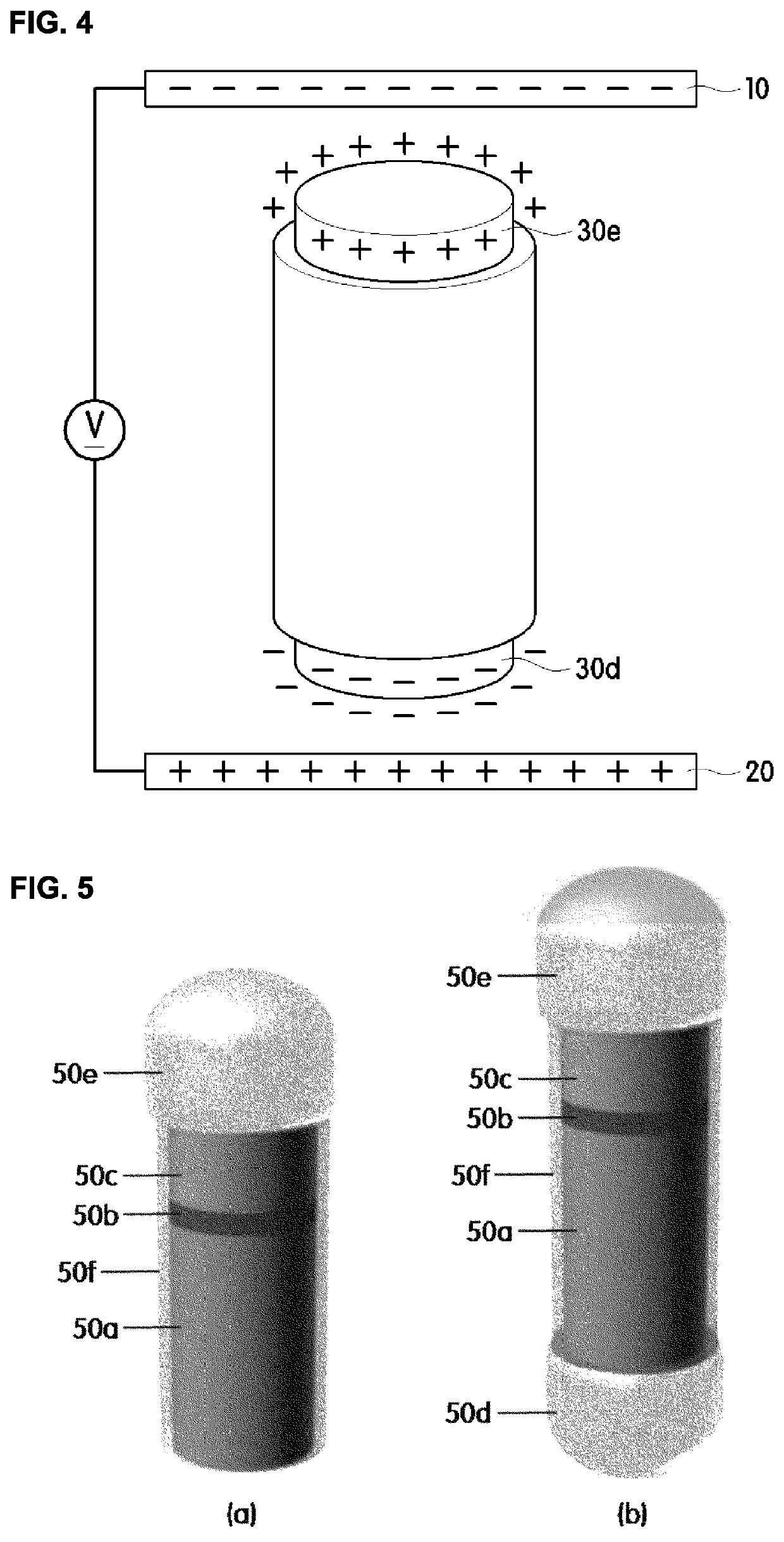
[0053]As described above, since nano-scale light-emitting diode (LED) elements cannot be individually arranged and mounted in a target electrode region with human hands because of a limitation of a size of each of the nano-scale LED elements, it is very difficult to arrange and mount the nano-scale LED elements on the electrode as intended. In order to solve such a problem, the inventor of the present invention found that a nano-scale LED horizontal array assembly may be implemented in which nano-scale LED elements are self-aligned due to an influence of an electric field so that both ends of each of the elements are connected to two different electrodes when power is applied to an electrode line into which a solution containing the nano-scale LED elements is injected. However, the present inventor recognized that since the self-alignment of the n...


PUM

PropertyMeasurementUnit
diameteraaaaaaaaaa
lengthaaaaaaaaaa
thicknessaaaaaaaaaa

Abstract

The present invention relates to a nano-scale light-emitting diode (LED) element for a horizontal array assembly, a manufacturing method thereof, and a horizontal array assembly including the same, and more particularly, to a nano-scale LED element for a horizontal array assembly that can significantly increase the number of nano-scale LED elements connected to an electrode line, facilitate an arrangement of the elements, and implement a horizontal array assembly having a very good electric connection between an electrode and an element and a significant high quantity of light when a horizontal array assembly having the nano-scale LED elements laid in a length direction thereof and connected to the electrode line is manufactured, a manufacturing method thereof, and a horizontal array assembly including the same.

Description

TECHNICAL FIELDCross-Reference to Related Applications[0001]This application is a national phase application under 35 U.S.C. § 371 of International Application No. PCT / KR2015 / 012252, filed Nov. 13, 2015, which claims priority to Korean Patent Application No. 10-2014-0161067, filed Nov. 18, 2014, the contents of which applications are incorporated into the present application by reference.[0002]The present invention relates to a nano-scale light-emitting diode (LED) element for a horizontal array assembly, a method of manufacturing the same, and a horizontal array assembly including the same, and more particularly, to a nano-scale LED element for a horizontal array assembly that can significantly increase the number of nano-scale LED elements connected to an electrode line, facilitate an arrangement of elements thereof, and implement a horizontal array assembly having a very good electric connection between an electrode and an element and a significantly high quantity of light when a...

Claims


Application Information

Patent Timeline
Patent Type & Authority Patents(United States)
IPC IPC(8): H01L33/00H01L33/20H01L33/06H01L33/08H01L33/24H01L33/38H01L33/44B82B3/00H01L33/32
CPCH01L33/0075H01L33/06H01L33/08H01L33/20H01L33/24H01L33/38H01L33/44B82B3/0052H01L33/32H01L33/385H01L2224/95085H01L2933/0016H01L2933/0025F21S4/00H01L25/0753H01L33/62H01L2933/0066H01L25/075H01L33/005H01L33/02H01L33/48
Inventor SUNG, YEON GOOG
Owner SAMSUNG DISPLAY CO LTD
Why Eureka
Try Eureka