Cobalt filling of interconnects in microelectronics

a microelectronics and interconnection technology, applied in the field of electrolytic deposition chemistry, can solve problems such as voids and hillocks, electrical shorts, and detrimental to devices

Active Publication Date: 2021-05-04
MACDERMID ENTHONE INC
View PDF20 Cites 0 Cited by
  • Summary
  • Abstract
  • Description
  • Claims
  • Application Information

AI Technical Summary

Benefits of technology

[0009]Also described are methods for filling submicron features of a semiconductor integrated circuit device by electrodeposition from the aforesaid compositions.

Problems solved by technology

Copper also has a tendency to migrate from one location to another when electrical current passes through interconnect features in service, creating voids and hillocks.
Such diffusion can be detrimental to the device because it can damage an adjacent interconnect line and / or cause electrical leakage between two interconnects resulting in an electrical short.
And the corresponding diffusion out of the interconnect feature can disrupt electrical flow.
The build-up process such as barrier and seed layers, prior to damascene copper electroplating, now suffers from disadvantages that are becoming more pronounced as the demand for higher aspect ratio features and quality electronic devices increases.
However, because of a higher resistivity of cobalt deposits, such processes have not previously offered a satisfactory alternative to electrodeposition of copper in filling vias or trenches to provide the primary interconnect structures.

Method used


Image

  • Cobalt filling of interconnects in microelectronics

Examples


example 1

[0043]An electrolytic cobalt deposition composition was prepared with the following components:

[0044]CoSO4— 7.75 g / L (concentration with reference to anhydrous cobalt sulfate)

[0045]H3BO3— 31.92 g / L

[0046]bis-(sodium sulfopropyl) disulfide (SPS)—10 mg / L

[0047]propargyl alcohol—15 mg / L

[0048]968.8 g water to balance to 1 L

[0049]pH adjusted to 2.9

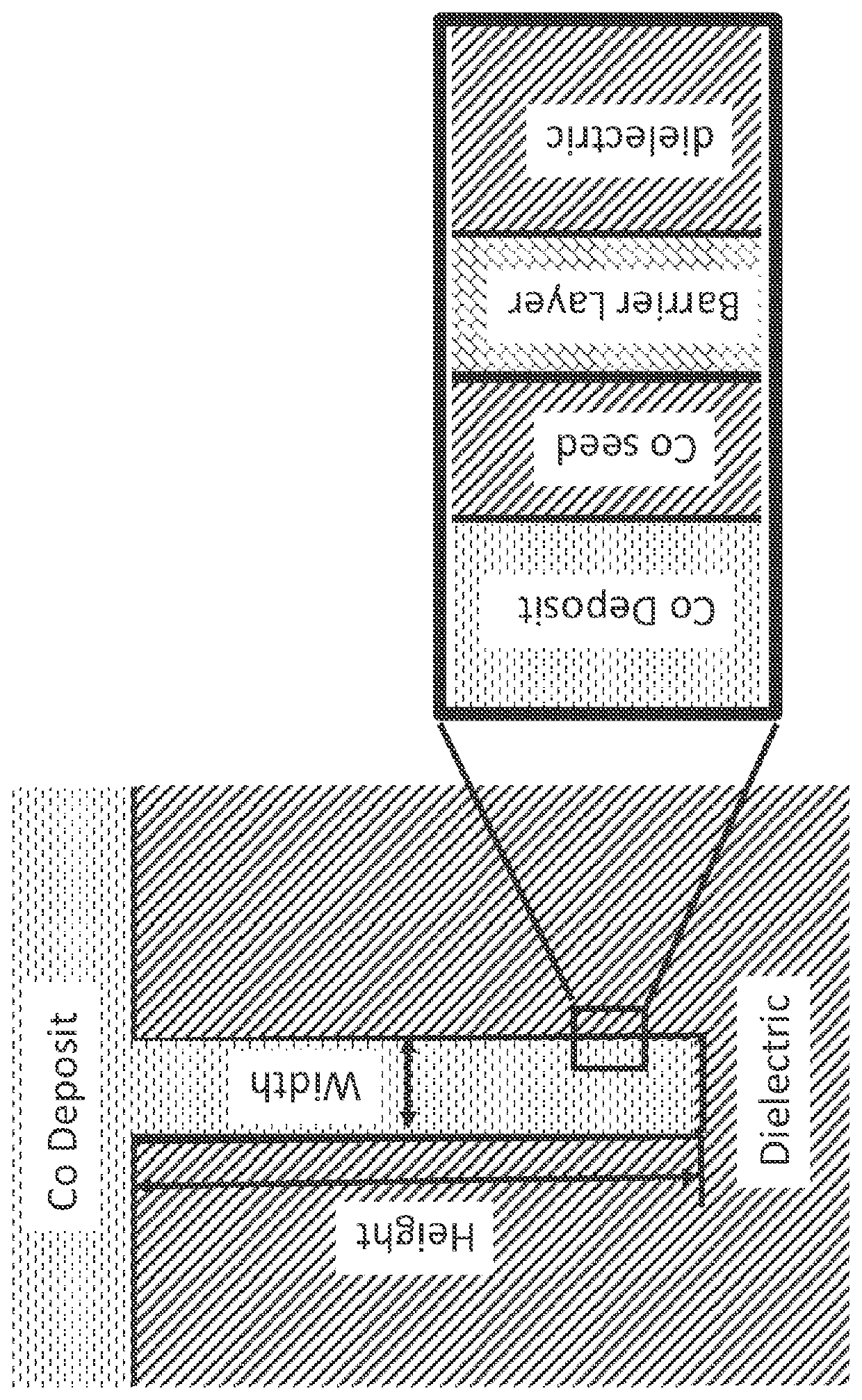
[0050]This composition may be used to fill a feature having a 12 nm top opening, a 7 nm middle width, a 2 nm bottom width, and a depth of 130 nm at a current density of 4 mA / cm2 for 3 minutes at room temperature and a rotation rate of 100 rpm.


PUM

PropertyMeasurementUnit
vol. %aaaaaaaaaa
internal tensile stressesaaaaaaaaaa
concentrationaaaaaaaaaa

Abstract

Processes and compositions for electroplating a cobalt deposit onto a semiconductor base structure comprising submicron-sized electrical interconnect features. In the process, a metalizing substrate within the interconnect features is contacted with an electrodeposition composition comprising a source of cobalt ions, an accelerator comprising an organic sulfur compound, an acetylenic suppressor, a buffering agent and water. Electrical current is supplied to the electrolytic composition to deposit cobalt onto the base structure and fill the submicron-sized features with cobalt. The process is effective for superfilling the interconnect features.

Description

FIELD OF THE INVENTION[0001]The compositions and processes described herein generally relate to electrolytic deposition chemistry and a method for depositing cobalt and cobalt alloys; and more specifically to additives and overall compositions for use in an electrolytic plating solution and a method for cobalt-based metallization of interconnect features in semiconductor substrates.BACKGROUND OF THE INVENTION[0002]In damascene processing, electrical interconnects are formed in an integrated circuit substrate by metal-filling of interconnect features such as vias and trenches formed in the substrate. Copper is a preferred conductor for electronic circuits. But when copper is deposited on a silicon substrate, it can diffuse rapidly into both the substrate and dielectric films such as SiO2 or low k dielectrics. Copper also has a tendency to migrate from one location to another when electrical current passes through interconnect features in service, creating voids and hillocks. Copper c...

Claims


Application Information

Patent Timeline
Patent Type & Authority Patents(United States)
IPC IPC(8): C25D3/16C25D7/12C25D3/56C25D5/18
CPCC25D7/12C25D3/16C25D3/562C25D5/18C25D7/123
Inventor COMMANDER, JOHNPANECCASIO, JR., VINCENTROUYA, ERICWHITTEN, KYLESUN, SHAOPENGHAN, JIANWEN
Owner MACDERMID ENTHONE INC
Why Eureka
Try Eureka