Device having a substrate configured to be thermoformed coupled to an electrically conductive member

a technology of electrically conductive components and substrates, applied in the direction of printed circuit aspects, printed circuit dielectrics, domestic articles, etc., can solve the problems of affecting the electrical conductivity of the substrate, so as to improve the electrical conductivity of the electrical conductive member and satisfy the electrical conduction

Active Publication Date: 2021-05-25
COMMISSARIAT A LENERGIE ATOMIQUE ET AUX ENERGIES ALTERNATIVES
View PDF51 Cites 0 Cited by
  • Summary
  • Abstract
  • Description
  • Claims
  • Application Information

AI Technical Summary

Benefits of technology

[0007]It is an aim of the invention to provide a device intended to be deformed, notably by thermoforming, and comprising an electrically conductive member capable of having a satisfactory electrical conduction even after it has been deformed. The aim is thus to find a solution which makes it possible to respond to the issue of improving the electrical conductivity of the electrical conductive member, in particular when the latter is intended to be thermally and mechanically stressed.

Problems solved by technology

The deposition techniques of microelectronics are appropriate but expensive and limited to rigid supports.
The polymer makes possible a degree of flexibility but has the disadvantage of damaging the electrical conductivity and of creating parasitic capacitances.
The result of this is the formation of antennas of mediocre quality since the quality factor of an antenna is dependent on its electrical conductivity.
Depending on the shape related to the thermoforming, this results in an issue of electrical continuity within the track as the latter may have, after thermoforming, breaks or cracks harmful to the conduction of the current.

Method used


Image

  • Device having a substrate configured to be thermoformed coupled to an electrically conductive member
  • Device having a substrate configured to be thermoformed coupled to an electrically conductive member
  • Device having a substrate configured to be thermoformed coupled to an electrically conductive member

Examples


Embodiment Construction

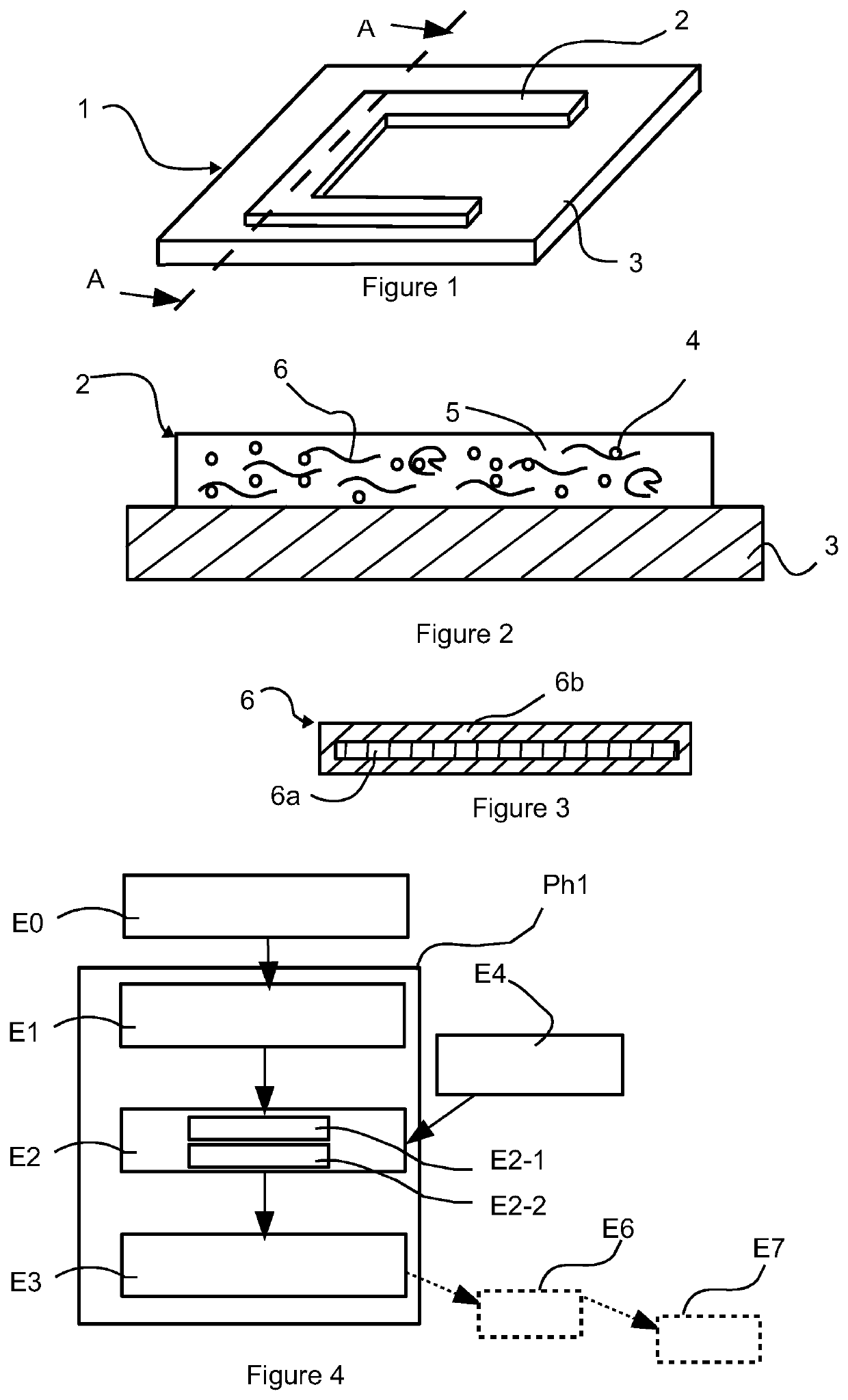
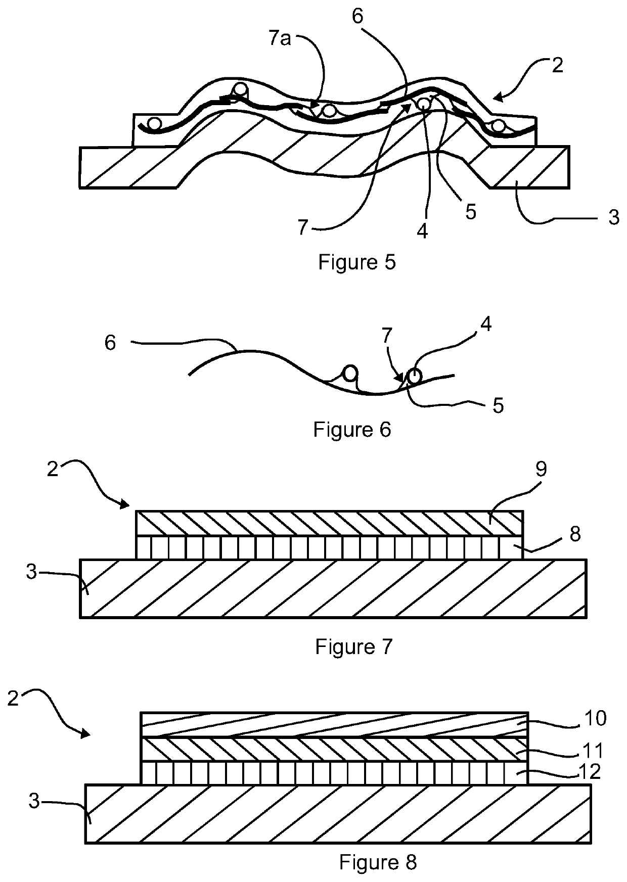
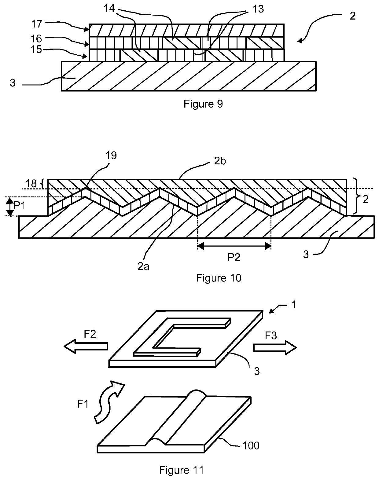
[0039]A description is given below of a device intended to be deformed, notably thermoformed, and which makes it possible to ensure, even after the deformation, an electrical continuity within an electrically conductive member, or track, which the device comprises. After thermoforming, reference is made to thermoformed device. For this, the electrically conductive member judiciously comprises electrically conductive particles, an electrically conductive material, in particular intended to undergo melting during the thermoforming or subsequent to the thermoforming, and electrically conductive elements of elongated shape which will make it possible to ensure the electrical continuity between electrically conductive particles which are moving away during the deformation, notably thanks to the melting of the electrically conductive material. In particular, this melting of the electrically conductive material makes it possible, in combination with the elongation of the elements of elonga...


PUM

PropertyMeasurementUnit
lengthaaaaaaaaaa
thicknessaaaaaaaaaa
thicknessaaaaaaaaaa

Abstract

The device intended to be thermoformed comprises a substrate capable of being thermoformed and an electrically conductive member integral with the said substrate. The electrically conductive member comprises: electrically conductive particles, an electrically conductive material, electrically conductive elements of elongated shape. The electrically conductive material has a melting point which is strictly less than the melting point of the electrically conductive particles and than the melting point of the elements of elongated shape.

Description

FIELD OF THE INVENTION[0001]The field of the invention relates to thermoformable devices and more particularly to the thermoforming of a device equipped with an electrically conductive member capable of having electrical conduction after thermoforming.STATE OF THE ART[0002]In the field of electronics, it is known to form electrically conductive tracks which can delimit, at least in part, an antenna or also an inductance. The deposition techniques of microelectronics are appropriate but expensive and limited to rigid supports. There thus exists a need to reduce the costs of the operations for forming electrically conductive tracks and to make possible the formation of such tracks on supports which are, for example, flexible and capable of being thermoformed according to requirements.[0003]From the perspective of reducing the costs, solutions have been developed for printing electrically conductive tracks based on inks. Apart from the advantage of reducing the costs, such inks can als...

Claims


Application Information

Patent Timeline
Patent Type & Authority Patents(United States)
IPC IPC(8): H05K3/10H05K1/09H05K3/00B29C51/10B29C51/14B29C51/42H05K3/12B29K105/00B29L9/00B29L31/34H01Q1/38
CPCH05K3/10B29C51/10B29C51/14B29C51/421H05K1/092H05K3/0014B29K2105/256B29K2995/0005B29L2009/005B29L2031/3456H01Q1/38H05K3/1283H05K2201/0129H05K2201/026H05K2201/0272H05K2201/09218H05K2201/10098H05K2203/0425H05K2203/1105H05K2203/1121
Inventor BENWADIH, MOHAMMED
Owner COMMISSARIAT A LENERGIE ATOMIQUE ET AUX ENERGIES ALTERNATIVES
Why Eureka
Try Eureka