
Biodegradable electroconducting nanowire, method of manufacture and uses thereof

a nanowire, biodegradable technology, applied in the field of electroconducting nanowires, can solve the problems of inorganic nanowires that are obviously not biodegradable, lack of data in the literature on potential nanoscopic applications of this type of nanowire, and presence in cellular tissues

Active Publication Date: 2014-05-29
COMMISSARIAT A LENERGIE ATOMIQUE ET AUX ENERGIES ALTERNATIVES
View PDF0 Cites 5 Cited by
  • Summary
  • Abstract
  • Description
  • Claims
  • Application Information

AI Technical Summary

Benefits of technology

The patent text describes a method for creating conductive nanowires using hybrid organic / inorganic materials. These nanowires can be used to create a metal sheath around DNA strands or amyloid fibres, which ensures good electrical conductivity. These nanowires are stable and can be purified, making them useful for creating functional proteins. The method also allows for the formation of amyloid fibres by inducing denaturation of peptides and the use of chimeric proteins.

Problems solved by technology

Nevertheless, these nano-objects raise numerous questions in terms of public health.
In fact, it is known that they can enter the body through cutaneous, digestive and respiratory routes, and their presence in cellular tissues could prove, in the long term, to be dangerous and all the more so in that the nano-objects proposed to date are not biodegradable or, in the very best of cases, are only very partially biodegradable.
These inorganic nanowires are obviously not biodegradable.
There exists moreover little data in the literature on potential nanoscopic applications of this type of nanowire.
In particular, they are not biodegradable and their applications are almost exclusively macroscopic.

Method used


Image

  • Biodegradable electroconducting nanowire, method of manufacture and uses thereof
  • Biodegradable electroconducting nanowire, method of manufacture and uses thereof
  • Biodegradable electroconducting nanowire, method of manufacture and uses thereof

Examples


example 1

Formation of Electroconducting Nanowires According to the Invention

[0116]Electroconducting nanowires are formed by expression, in cells of Escherichia coli, of chimeric proteins each comprising the aforementioned sequence of amino acids SEQ ID NO: 9, to which has been added, on the side of the C-terminal asparagine residue of this sequence, a tag composed of 6 histidine residues intended to enable the purification by IMAC (Immobilized Metal Affinity Chromatography), and, more specifically on a nickel column, of the chimeric proteins thereby expressed.

[0117]Chimeric proteins thus have the following sequence of amino acids:

(sequence ID NO: 10)MAIWQCTVCGYKYDEDKEKKKFEDLPADYKCPVCGAKKEMFKKSMEIDAIVGRNSAKDIRTEERARVQLGNVVTAAALHGGIRISDQTTNSVETVVGKGESRVLIGNEYGGKGFWDNHHHHHH.

[0118]To do this, the nucleotide sequence encoding for the peptide with prion domain:

(sequence ID NO: 11)ATGGAGATCGACGCGATTGTGGGAAGGAATTCCGCCAAGGATATCAGAACAGAGGAACGTGCAAGGGTCCAGCTCGGCAATGTTGTCACTGCGGCAGCCCTACATGGTGGGATCCGTAT...

example 2

Characterisation and Properties of Electroconducting Nanowires According to the Invention

[0140]2.1. Fibrillar Structure of the Nanowires

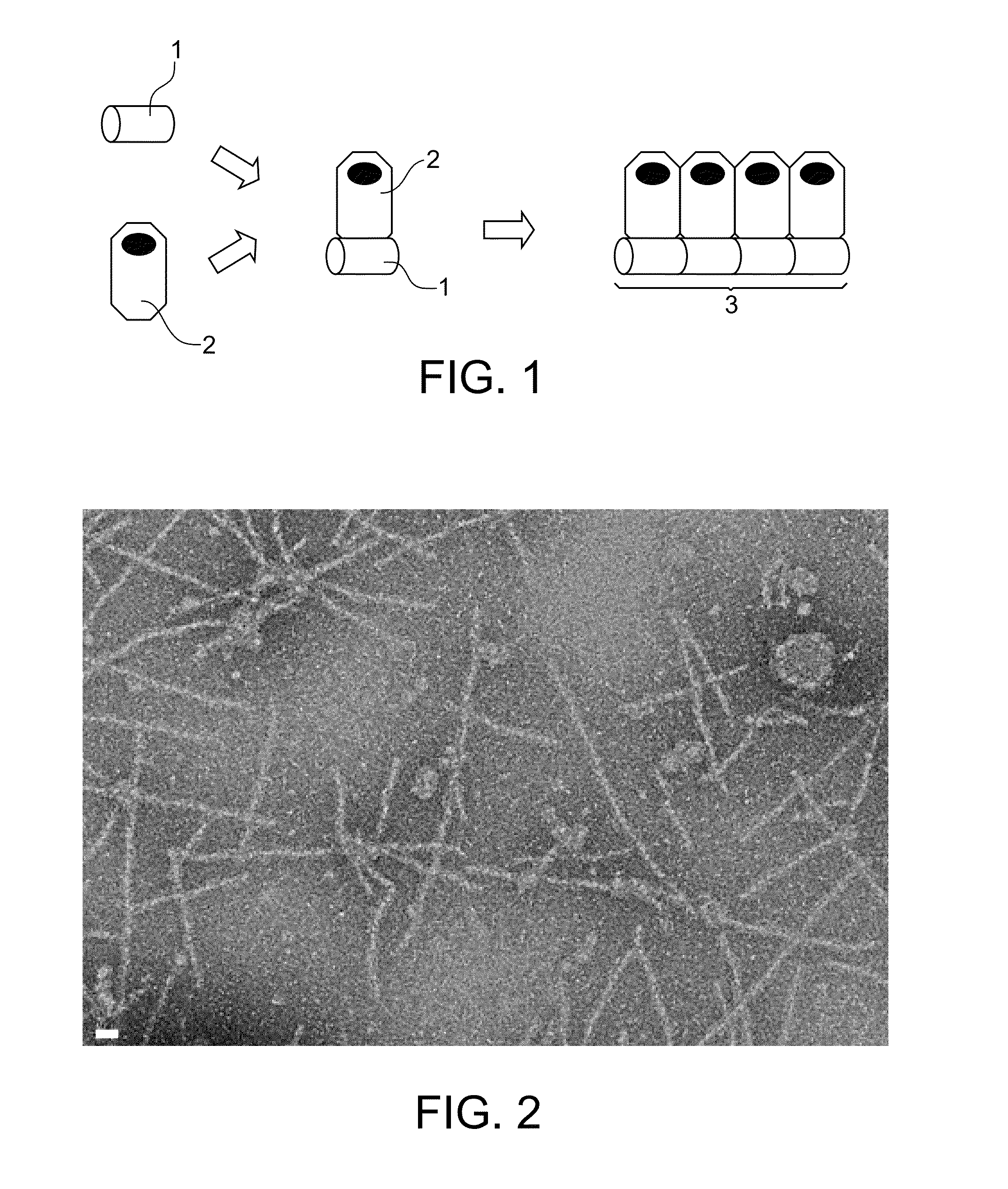
[0141]FIG. 3 shows an image taken in transmission electron microscopy by negative coloration with uranyl salt of the nanowires obtained in example 1 and on which the scale, which is represented by the rectangle situated in the bottom left hand corner of this image, corresponds to 20 nm.

[0142]This figure shows that the nanowires have, as expected, a fibrillar structure and that they have substantially a thickness of 8 nm for a length ranging from 200 nm to 2 μm.

[0143]2.2. Electroconducting Properties of Nanowires

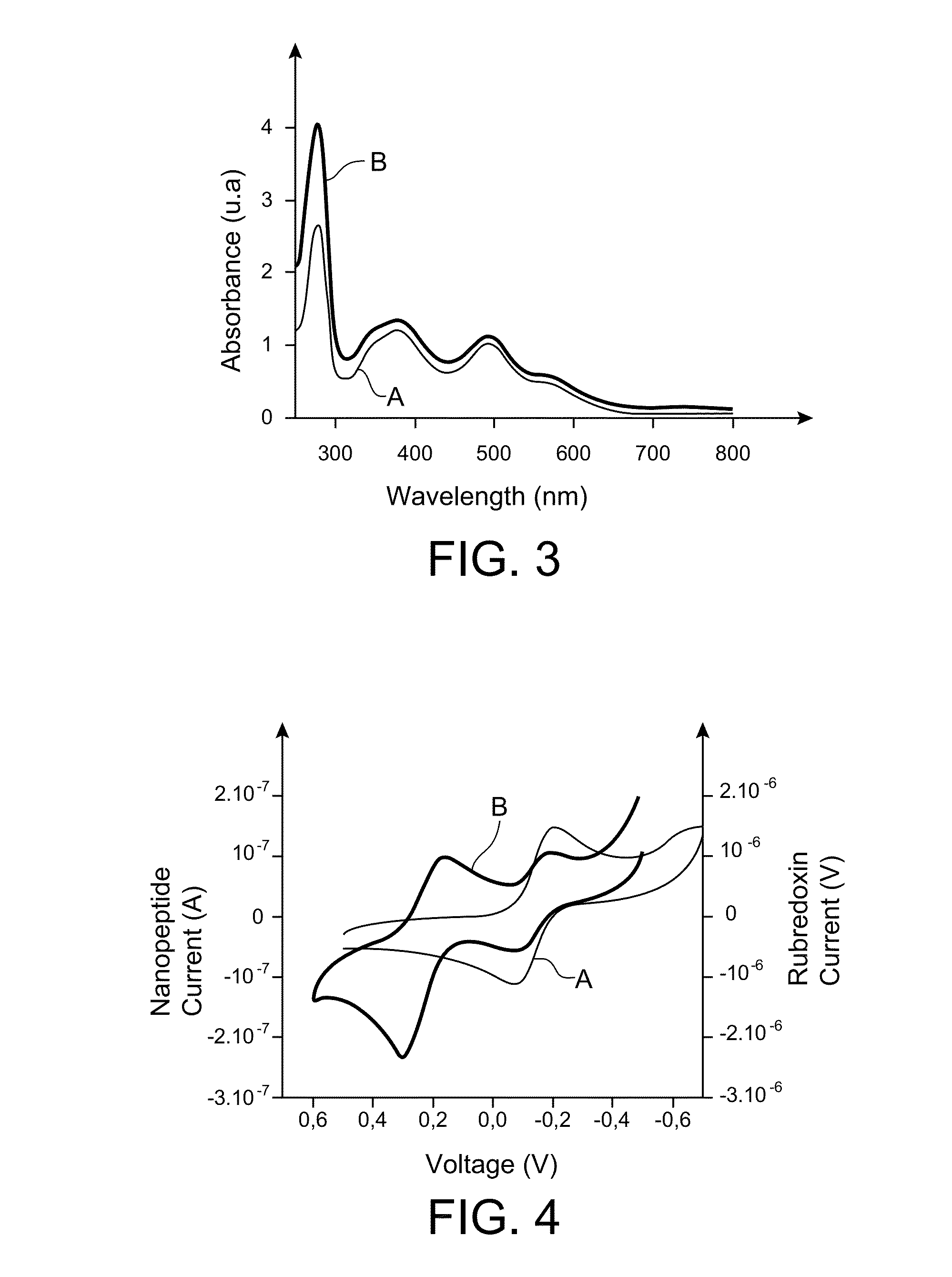
[0144]In order that the nanowires obtained in example 1 above can conduct electrons on either side of the amyloid fibre which constitutes them, it is important that the peptide sequences derived from the rubredoxin of Methanococcus voltae, which functionalize this amyloid fibre, are correctly folded on their iron-sulphur centre.

[0145]The rubr...


PUM

PropertyMeasurementUnit
Fractionaaaaaaaaaa
Biodegradabilityaaaaaaaaaa

Abstract

The subject matter of the invention is an electroconducting nanowire, comprising an amyloid fibre which results from the self-assembling of peptides comprising a prion domain or a derivative of this domain and which is functionalized by electron transporting peptides, each comprising amino acids bound to one or more atoms of iron.Its subject matter is also a method of manufacturing this nanowire as well as the uses of said nanowire.Uses: manufacture of sensors for the detection of chemical or biological species, of nano-batteries, of radio-identification systems, of molecular memory systems, etc.

Description

TECHNICAL FIELD[0001]The present invention belongs to the technical field of electroconducting nanowires, their manufacture and their uses.[0002]More specifically, it relates to nanowires which, apart from having electrical conduction properties, are biodegradable, in other words that they may be entirely degraded by living organisms, and are provided with self-organisation properties on both a nanoscopic and macroscopic scale.[0003]The invention also relates to a method making it possible to manufacture said nanowires as well as to the uses of said nanowires.[0004]Given their remarkable properties, the nanowires according to the invention are likely to find numerous applications, both nanoscopic and macroscopic.[0005]For instance, they may in particular be used in sensors, and in particular sensors intended to detect chemical or biological species, in nanobatteries, and in particular in nanobatteries intended to transform solar energy into electricity, in radio-identification syste...

Claims


Application Information

Patent Timeline
IPC IPC(8): C07K14/00
CPCB82Y30/00C07K14/4711C07K2319/735B82Y40/00C07K14/001
Inventor FORGE, VINCENTHORVATH, CHRISTOPHEFONTECAVE, MARCDURAFFOURG, NICOLAS
Owner COMMISSARIAT A LENERGIE ATOMIQUE ET AUX ENERGIES ALTERNATIVES
Learn More