Low parasitic inductance power module and double-faced heat-dissipation low parasitic inductance power module

a power module and low parasitic inductance technology, applied in the field of power modules, can solve the problems of large package volume, heavy weight, and inability to meet the requirements of high power density and light weight, and achieve the effect of reducing the parasitic inductance of the loop, reducing the volume of the power module, and saving costs

Active Publication Date: 2021-10-05
YANGZHOU GUOYANG ELECTRONICS CO LTD
View PDF7 Cites 0 Cited by
  • Summary
  • Abstract
  • Description
  • Claims
  • Application Information

AI Technical Summary

Benefits of technology

[0006]Object of the present invention: aiming at the defects in the prior art, the present invention is intended to provide a low parasitic inductance power module with small volume, light weight and small parasitic inductance, and a double-sided heat-dissipation low parasitic inductance power module.
[0028]Beneficial effects: according to the present invention, the top metal insulating substrate and the bottom metal insulating substrate are stacked, the chips are sintered on the faces of both the top metal insulating substrate and the bottom metal insulating substrate opposite to each other, and the welding portion of the output power terminal is also arranged between the top metal insulating substrate and the bottom metal insulating substrate; in this way, the stacked arrangement of the chips and the electrodes can greatly reduce a parasitic inductance of a loop, decrease a volume of the power module, save costs, lighten a weight, and is particularly suitable for packaging a SiC power chip; meanwhile, the power terminals of the chips in the power module all adopt a large-area sintering structure, thus greatly reducing the module failure risk caused by the failure of bonding wires when the bonding wires are used, fully improving an overcurrent capability and improving a reliability of the module. In addition, heat sinks may be arranged on both sides of the power module, so that the thermal resistance of the power module can be reduced, or the heat sink may be arranged at the bottom of the power module, and the top of the of the power module is connected to the heat sink by the heat pipe for double-faced heat dissipation, so that the structure of the heat radiator can be further simplified and the volume of the heat radiator can be compressed while the heat dissipation efficiency of the power module is ensured.

Problems solved by technology

The present power module in power electronics has a large package volume and a heavy weight, which does not meet the requirements of high power density and light weight in the fields of electromobiles, aerospace and the like.
The power module in power electronics with a larger volume often has a larger parasitic inductance, which will result in a larger overshoot voltage and increase losses, and also limit the application of the power module in a high switching frequency occasion.
A SiC power electronic device has the characteristics of high frequency, high temperature and high efficiency, but the present power module has a larger parasitic inductance, which limits the performance implementation of the SiC.
In addition, with the continuous upgrading of the power density at an application end, a package structure of the present power module has hindered the further improvement of the power density, and a more effective heat dissipation structure has to be developed to meet the increasing demand of the power density.
In addition, a power terminal and a control terminal are only connected with a first lining plate, so that the arrangement is not flexible enough, an area of the lining plate cannot be further reduced, and losses are increased due to a long current path.

Method used


Image

  • Low parasitic inductance power module and double-faced heat-dissipation low parasitic inductance power module
  • Low parasitic inductance power module and double-faced heat-dissipation low parasitic inductance power module
  • Low parasitic inductance power module and double-faced heat-dissipation low parasitic inductance power module

Examples


embodiment 1

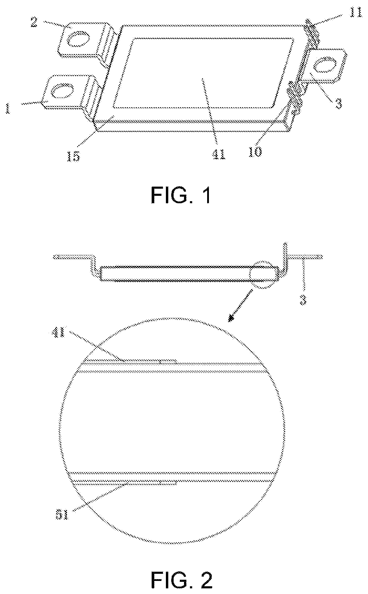
[0065]According to the invention, a switch chip and a freewheel diode chip of a relative bridge arm are stacked, so that a commutating loop path is shortest, thereby greatly reducing a parasitic inductance of the loop. The purpose of double-faced heat dissipation is achieved by arranging heat dissipation paths on both sides of the stacked chips, thus further reducing a thermal resistance of a power module.

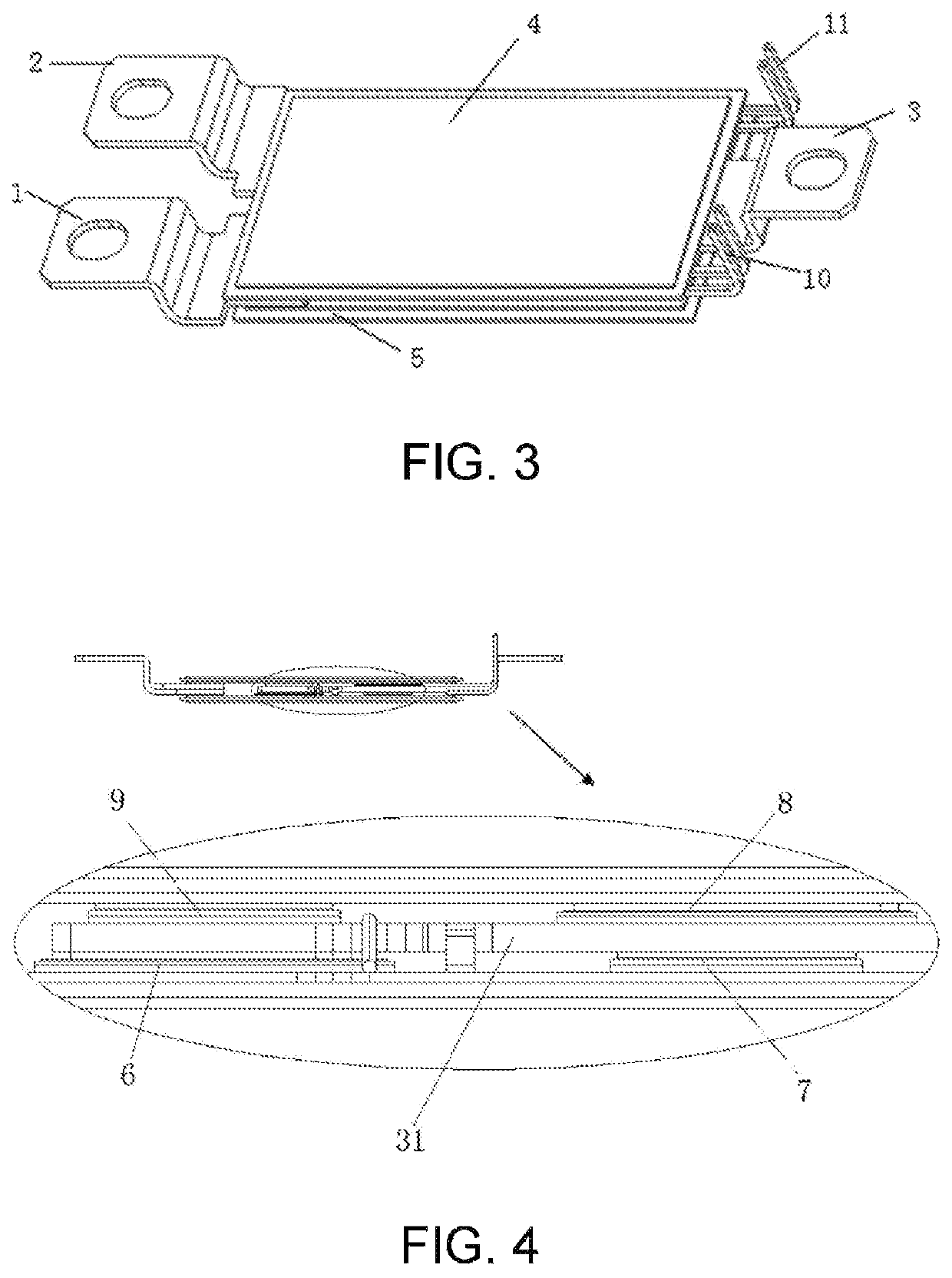
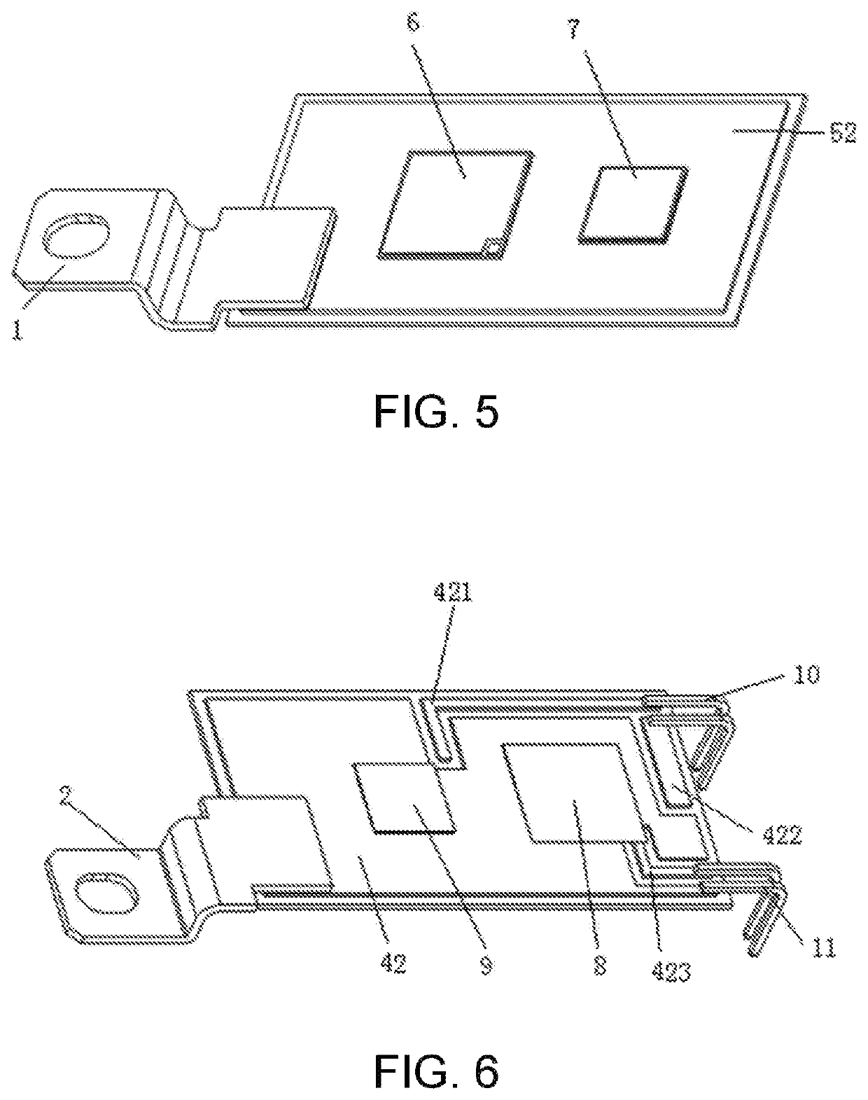
[0066]As shown in FIG. 1, a double-faced heat-dissipation low parasitic inductance power module includes a positive power terminal 1, a negative power terminal 2, an output power terminal 3, a bottom metal insulating substrate 5 connected with the positive power terminal 1, a top metal insulating substrate 4 connected with the negative power terminal 2, an upper half-bridge driving terminal 10, a lower half-bridge driving terminal 11 and a plastic package shell 15 used for encapsulating. The positive power terminal 1 in the embodiment is sintered on the bottom metal insulating subs...

embodiment 2

[0076]As shown in FIG. 14, the structure of this embodiment is basically the same as that of Embodiment 1, but differs in that the welding portion of the output power terminal 3 in the embodiment is a matrix 311 at a position contacted with the chip, and is a three-layer structure at a position not contacted with the chip, the matrix 311 is located in a middle layer, and fillers 312 are located at upper and lower sides. The matrix 311 is metal molybdenum or tungsten copper with small thermal expansion coefficients, and the filler 312 is metal silver with good conductivity.

[0077]In this embodiment, the power chip is sintered on the molybdenum matrix 311 of the output electrode, and a groove is machined in a part of the output electrode that is not contacted with the chip, and the groove is filled with silver. The thermal expansion coefficient of the metal molybdenum is generally one third of that of copper, which is close to that of the chip. During the operation of the power module,...

embodiment 3

[0078]As shown in FIG. 15, the structure of this embodiment is basically the same as that of Embodiment 1, but differs in that a stress buffer layer 14 is filled between the welding portion 31 of the output power terminal 3 and the chip, the welding portion 31 of the output power terminal 3 is metallic copper, and the stress buffer layer 14 is metallic molybdenum or tungsten copper.

[0079]The output electrode is made of pure copper. Due to a larger difference in thermal expansion between the copper and the chip, in order to improve the long-term reliability of the pad layer 16, the stress buffer layer 14 is added between the chip and the output electrode for transition in this embodiment, i.e., metal molybdenum or tungsten copper is sintered on the surface of the chip, and then molybdenum or tungsten copper is sintered on the output electrode.


PUM


Abstract

A low parasitic inductance power module, which includes an input power terminal, an output power terminal, a top metal insulating substrate, a bottom metal insulating substrate and a plastic package shell, wherein the input power terminal includes a positive power terminal and a negative power terminal, the top metal insulating substrate and the bottom metal insulating substrate are stacked, chips are sintered on faces of both the top metal insulating substrate and the bottom metal insulating substrate opposite to each other, and the positive power terminal, the negative power terminal, and the output power terminal are all electrically connected with the chips; and the output power terminal includes a welding portion and a connecting portion located outside the plastic package shell, and the welding portion is located between the top metal insulating substrate and the bottom metal insulating substrate.

Description

CROSS-REFERENCE TO RELATED APPLICATION[0001]This application is a 371 of international application of PCT application serial no. PCT / CN2017 / 090248, filed on Jun. 27, 2017, which claims the priority benefit of China application no. 201710448407.4, filed on Jun. 14, 2017. The entirety of each of the above mentioned patent applications is hereby incorporated by reference herein and made a part of this specification.BACKGROUNDTechnical Field[0002]The present invention relates to a power module in power electronics, and more particularly, to a low parasitic inductance power module and a double-faced heat-dissipation low parasitic inductance power module.Description of Related Art[0003]A power electronics technology plays a very important role in the rapidly developed industrial field today. As a representative of the power electronics technology, a power module in power electronics has been widely used in electromobiles, photovoltaic power generation, wind power generation, industrial fr...

Claims


Application Information

Patent Timeline
Patent Type & Authority Patents(United States)
IPC IPC(8): H01L25/07H01L23/538H01L23/498H01L23/051H01L23/49H01L23/31H01L23/367H01L23/427H01L23/14
CPCH01L25/071H01L23/051H01L23/142H01L23/3121H01L23/3672H01L23/427H01L23/49H01L23/49811H01L23/5385H01L23/3675H01L25/16H01L25/18H01L23/3677H01L23/3735H01L23/4334H01L2224/48227H01L2224/32225H01L2224/48091H01L2924/00014H01L2224/48472H01L2224/33181H01L2224/0603H01L2924/13091H01L2924/13055H01L24/83H01L2224/40137H01L24/40H01L2224/8484H01L24/84H01L24/32H01L2224/32245H01L2224/45099H01L2924/00H01L2224/73221
Inventor NIU, LIGANGWANG, YULINTENG, HESONGXU, WENHUI
Owner YANGZHOU GUOYANG ELECTRONICS CO LTD
Why Eureka
Try Eureka