Supercharge Your Innovation With Domain-Expert AI Agents!

Laser crystallization system and laser crystallization method

a laser crystallization and laser crystallization technology, applied in the direction of manufacturing tools, semiconductor/solid-state device testing/measurement, welding/soldering/cutting articles, etc., can solve the problems of significant cost loss, chamber and/or annealing window contamination,

Active Publication Date: 2021-11-09
SAMSUNG DISPLAY CO LTD
View PDF6 Cites 0 Cited by
  • Summary
  • Abstract
  • Description
  • Claims
  • Application Information

AI Technical Summary

Benefits of technology

[0004]Some embodiments provide a laser crystallization system preventing excimer laser from being irradiated to an amorphous silicon thin film when the amorphous silicon thin film is not normally deposited on a substrate or a concentration of hydrogen remaining in the amorphous silicon thin film is higher than a normal reference value.
[0005]Some embodiments provide a laser crystallization method preventing excimer laser from being irradiated to an amorphous silicon thin film when the amorphous silicon thin film is not normally deposited on a substrate or a concentration of hydrogen remaining in the amorphous silicon thin film is higher than a normal reference value.
[0023]In an embodiment, a laser crystallization method may further include reducing a concentration of hydrogen remaining in the amorphous silicon thin film when the light transmittance value is higher than the reference light transmittance value.
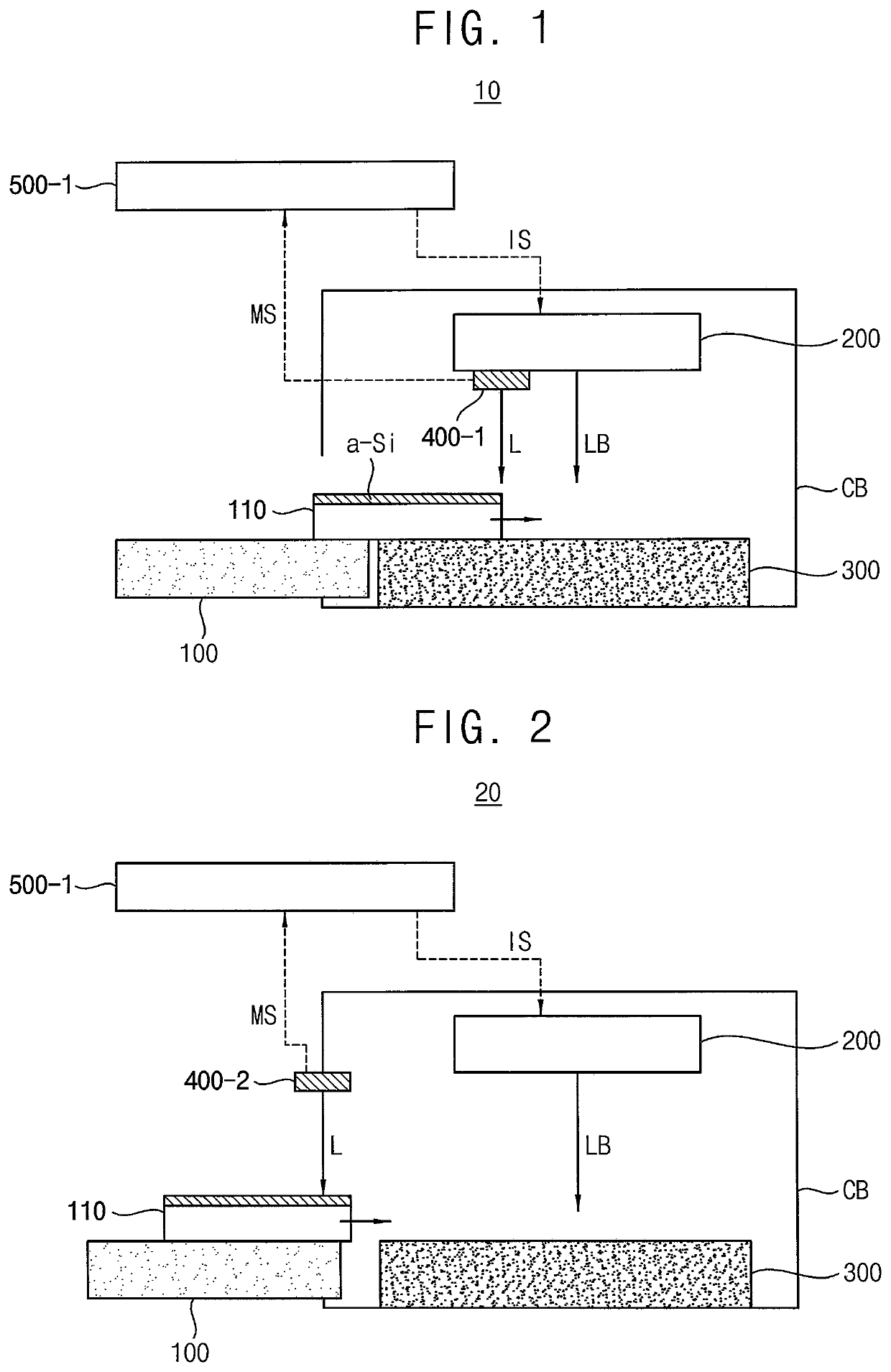
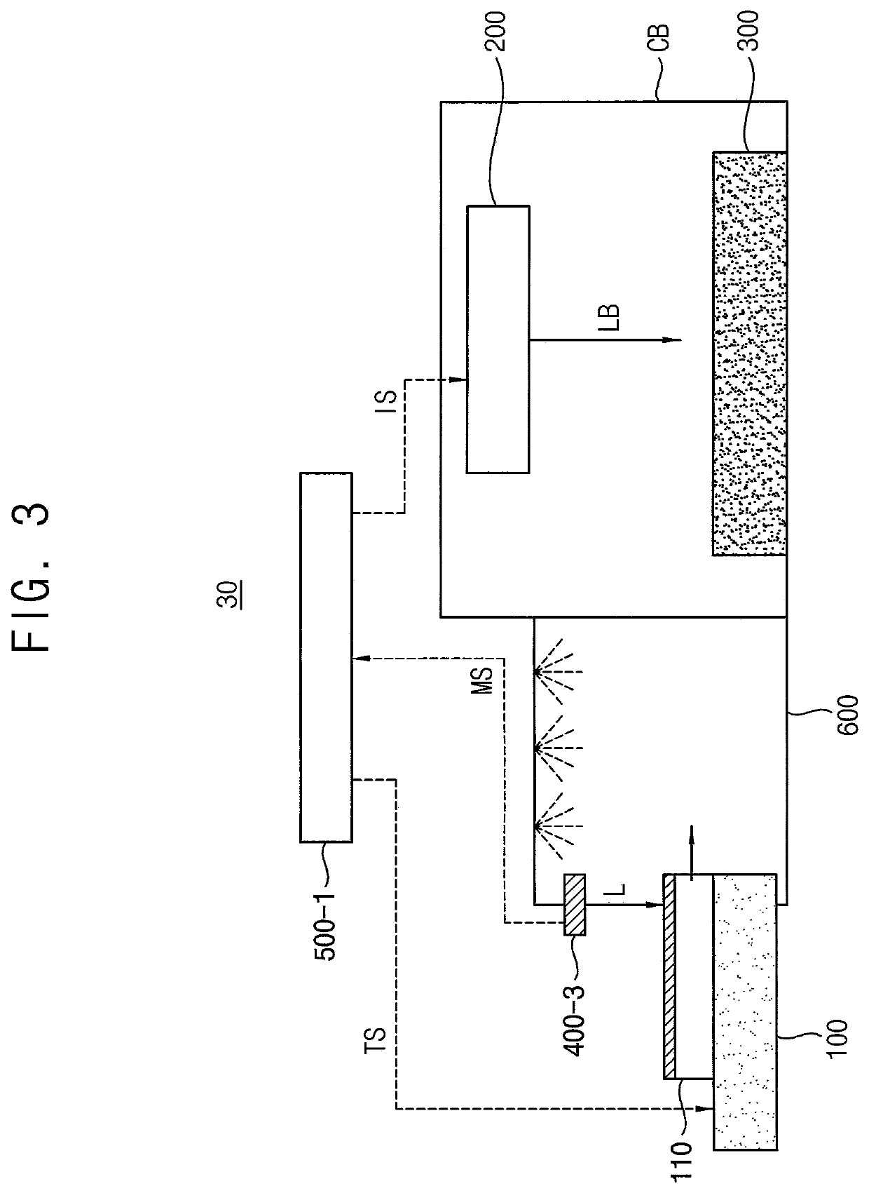
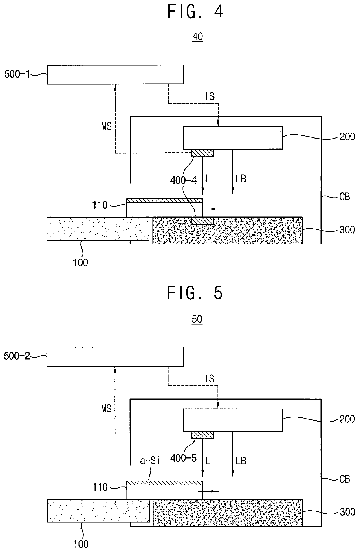
[0026]A laser crystallization system according to the embodiments may detect a defective substrate on which an amorphous silicon thin film is not normally deposited or whose concentration of hydrogen remaining in the amorphous silicon thin film is higher than a normal reference value in real time and may prevent a film floating phenomenon which may occur when an excimer laser is irradiated to the defective substrate, or when there is contamination of a chamber and / or an annealing window, by including a transfer part that transfers a substrate on which the amorphous silicon thin film is deposited into the chamber, a laser irradiation part that irradiates the excimer laser to the substrate for crystallization of the amorphous silicon thin film in the chamber, a stage that supports the substrate in the chamber, a measuring part that measures a light transmittance value of the substrate, and a controller that controls the laser irradiation part to irradiate the excimer laser to the substrate when the light transmittance value is equal to or lower than a reference light transmittance value and controls the laser irradiation part not to irradiate the excimer laser to the substrate when the light transmittance value is higher than the reference light transmittance value.
[0027]A laser crystallization system according to the embodiments may detect a defective substrate on which an amorphous silicon thin film is not normally deposited or whose concentration of hydrogen remaining in the amorphous silicon thin film is higher than a normal reference value in real time and may prevent a film floating phenomenon which may occur when an excimer laser is irradiated to the defective substrate, or when there is contamination of a chamber and / or an annealing window, by including a transfer part that transfers a substrate on which the amorphous silicon thin film is deposited into the chamber, a laser irradiation part that irradiates the excimer laser to the substrate for crystallization of the amorphous silicon thin film in the chamber, a stage that supports the substrate in the chamber, a measuring part that measures a light reflectance value of the substrate, and a controller that controls the laser irradiation part to irradiate the excimer laser to the substrate when the light reflectance value is equal to or higher than a reference reflectance value and controls the laser irradiation part not to irradiate the excimer laser to the substrate when the light reflectance value is higher than the reference reflectance value.
[0028]A laser crystallization method according to the embodiments may detect a defective substrate on which an amorphous silicon thin film is not normally deposited or whose concentration of hydrogen remaining in the amorphous silicon thin film is higher than a normal reference value in real time and may prevent a film floating phenomenon which may occur when an excimer laser is irradiated to the defective substrate, or when there is contamination of a chamber and / or an annealing window, by measuring a light transmittance value of a substrate on which an amorphous silicon thin film is deposited, comparing the light transmittance value to a reference light transmittance value, forming a polycrystalline silicon thin film by crystallizing the amorphous silicon thin film by irradiating an excimer laser to the substrate when the light transmittance value is equal to or lower than the reference light transmittance value, and controlling not to irradiate the excimer laser to the substrate when the light transmittance value is higher than the reference light transmittance value.

Problems solved by technology

In this method, when the excimer laser is irradiated to the amorphous silicon thin film when the amorphous silicon thin film is not normally deposited on the substrate or a concentration of hydrogen remaining in the amorphous silicon thin film is higher than a normal reference value, a film floating phenomenon may occur due to a portion where the amorphous silicon thin film is not deposited or due to hydrogen remaining in the amorphous silicon thin film, and a chamber and / or an annealing window may be contaminated.
When the chamber and / or the annealing window are contaminated, a significant cost loss may occur because laser crystallization facility checks (e.g., replacement of an annealing window, cleaning of a chamber, etc.) may be performed.

Method used


Image

  • Laser crystallization system and laser crystallization method
  • Laser crystallization system and laser crystallization method
  • Laser crystallization system and laser crystallization method

Examples


Embodiment Construction

[0037]Advantages and features of the disclosure and methods for accomplishing the same will be more clearly understood from embodiments described below with reference to the accompanying drawings. However, the disclosure is not limited to the following embodiments but may be implemented in various forms. The embodiments are provided only to complete the disclosure and to fully provide a person having ordinary skill in the art to which the disclosure pertains within the field of the disclosure.

[0038]It will be understood that when an element, such as a layer, film, region, substrate, or area is referred to as being “on” another element, it may be directly on or another element or intervening elements may be present therebetween.

[0039]In the drawings, sizes and thicknesses of elements may be enlarged for better understanding, clarity, and ease of description thereof. However, the disclosure is not limited to the illustrated sizes and thicknesses. In the drawings, for better understand...


PUM

PropertyMeasurementUnit
light transmittanceaaaaaaaaaa
concentrationaaaaaaaaaa
electron mobilityaaaaaaaaaa

Abstract

A laser crystallization system includes a transfer part that transfers a substrate on which an amorphous silicon thin film is deposited into a chamber, a laser irradiation part that irradiates an excimer laser to the substrate for crystallization of the amorphous silicon thin film in the chamber, a stage that supports the substrate in the chamber, a measuring part that measures a light transmittance value of the substrate, and a controller that controls the laser irradiation part to irradiate the excimer laser to the substrate when the light transmittance value is equal to or lower than a reference transmittance value and controls the laser irradiation part not to irradiate the excimer laser to the substrate when the light transmittance value is higher than the reference transmittance value.

Description

CROSS-REFERENCE TO RELATED APPLICATION(S)[0001]This application claims priority to and benefit of Korean Patent Application No. 10-2019-0067318, filed on Jun. 7, 2019 in the Korean Intellectual Property Office, the contents of which are incorporated herein by reference in its entirety.BACKGROUNDTechnical Field[0002]Embodiments relate generally to a laser crystallization system and a laser crystallization method that irradiate an excimer laser to an amorphous silicon thin film for crystallization of the amorphous silicon thin film to form a polycrystalline silicon thin film.Description of the Related Art[0003]As high performance of an element is required according to enlargement of a display device and high-definition of the display device, a high performance thin film transistor with high electron mobility is required. Accordingly, a polycrystalline silicon thin film transistor which has higher performance than performance of an amorphous silicon thin film transistor has been studie...

Claims


Application Information

Patent Timeline
Patent Type & Authority Patents(United States)
IPC IPC(8): H01L21/02
CPCH01L21/02686H01L21/02532H01L21/02422B23K26/352B23K26/354B23K2101/40B23K2103/56B23K26/127B23K26/123B23K26/082B23K26/03B23K26/083H01L21/02675H01L21/324H01L21/67276H01L22/12H01L22/30
Inventor SEO, JONGOHCHOI, JONGHOONKIM, JI-HWANSO, BYUNG SOOLEE, DONG-MINLEE, DONG-SUNG
Owner SAMSUNG DISPLAY CO LTD
Features
  • R&D
  • Intellectual Property
  • Life Sciences
  • Materials
  • Tech Scout
  • Unparalleled Data Quality
  • Higher Quality Content
  • 60% Fewer Hallucinations
Learn More