Method for fabricating microfluidic devices in fused silica by picosecond laser irradiation
a microfluidic device and fused silica technology, applied in manufacturing tools, laboratory glassware, welding/soldering/cutting articles, etc., can solve the problems of large difference in etch rate, unfavorable high-performance controllable fabrication of microchannels, and greatly reduced etch rate with respect to linearly polarized ligh
- Summary
- Abstract
- Description
- Claims
- Application Information
AI Technical Summary
Benefits of technology
Problems solved by technology
Method used
Image
Examples
embodiment 1
[0023]In the first embodiment of the present invention, the method comprises the following steps:
[0024]Step 1: Picosecond Laser Beam Irradiation
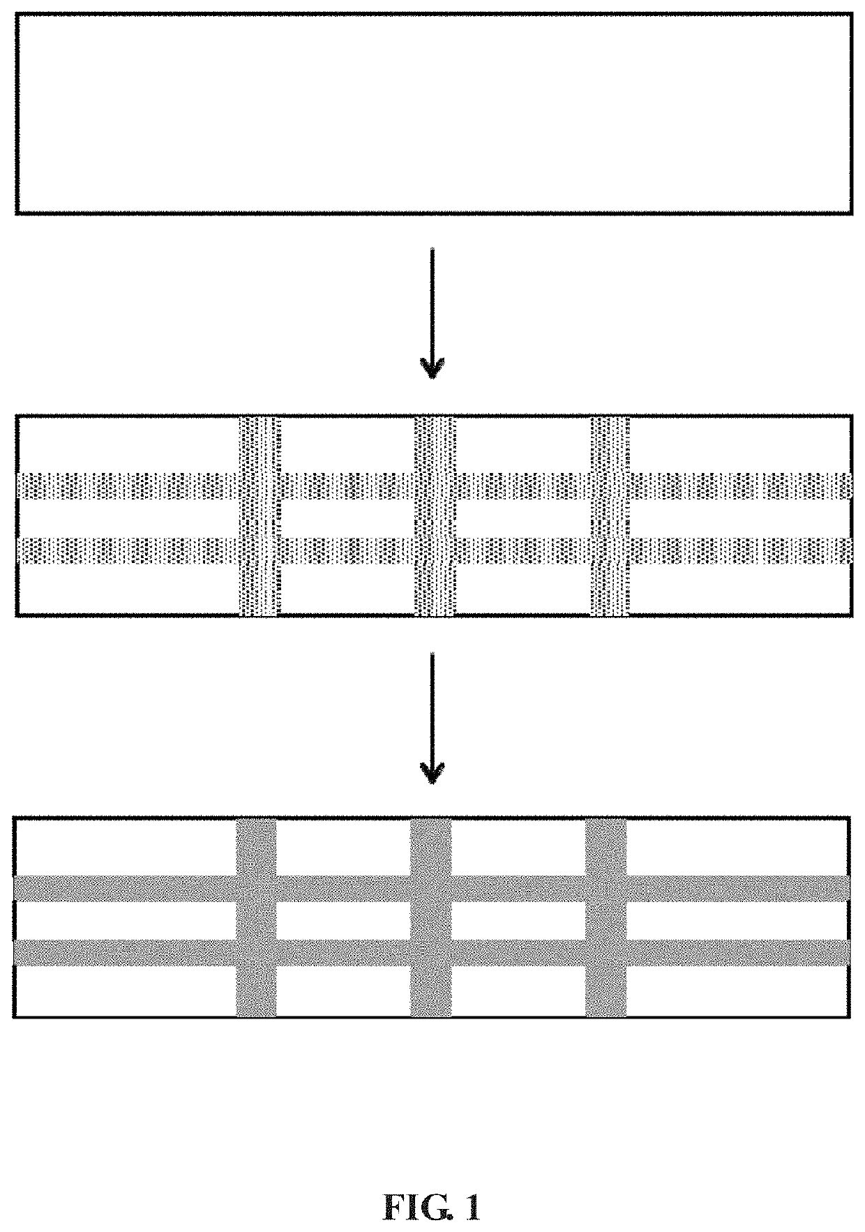
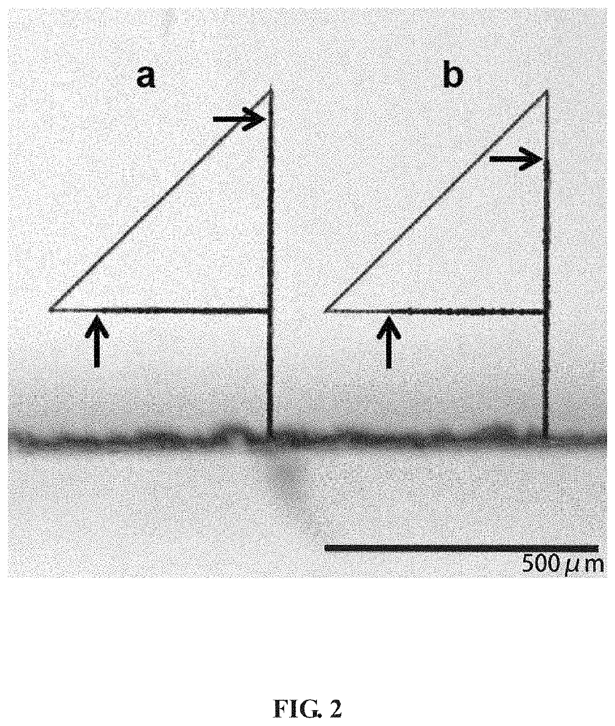
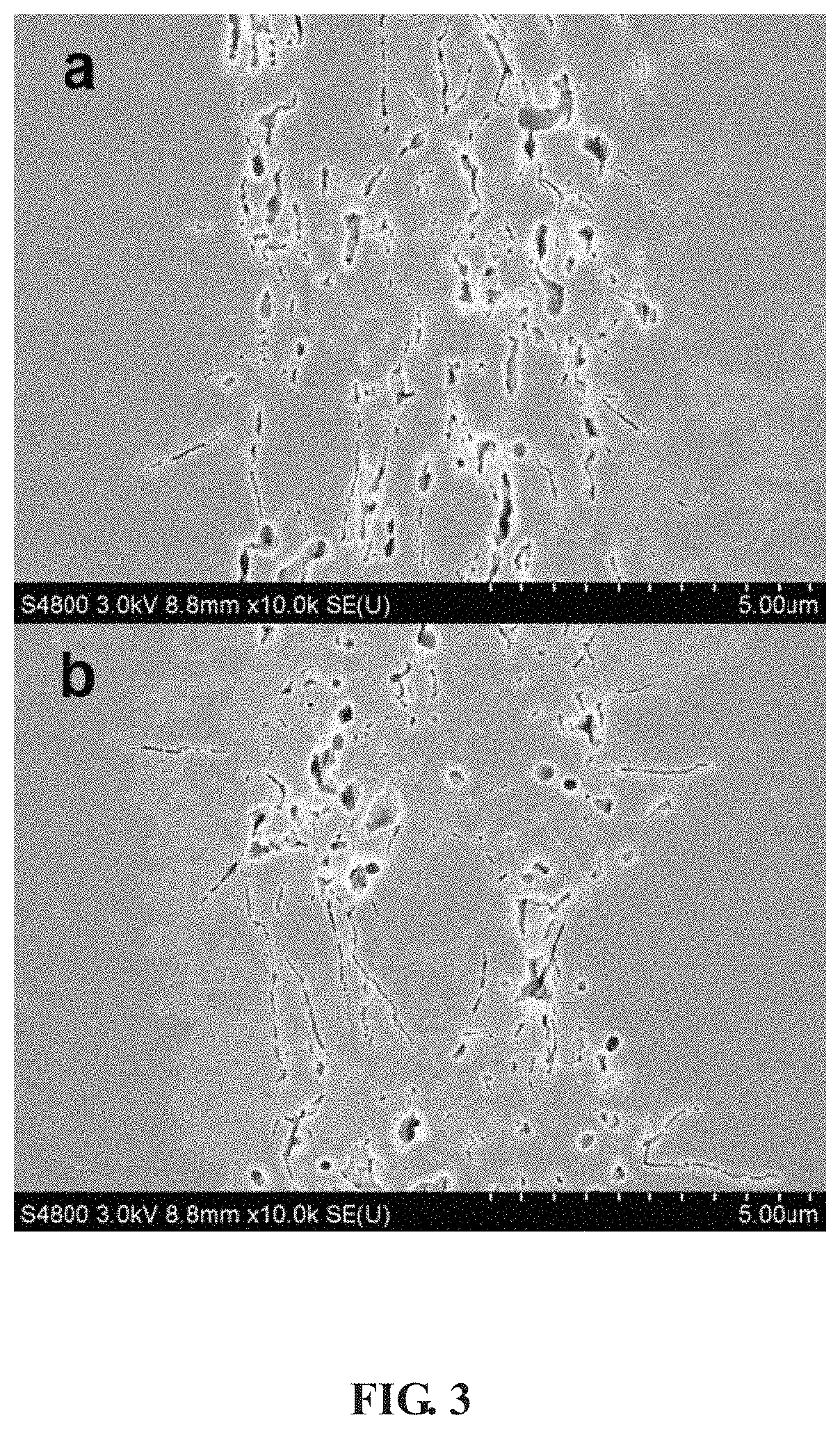
[0025]As shown in FIG. 1, fixing a clean glass sample of fused silica with a size of 20 mm×10 mm×2 mm and polished on six sides on a three-dimensional positioning stage; the laser operating at a center wavelength of 1026 nm, with a repetition rate of 50 kHz and a pulse width of 8 ps; focusing the laser beam at a depth of 300 μm below the surface of the glass substrate using a microscope objective with a numerical aperture of 0.45 (transmission rate is ˜30% for the beam). To evaluate the effect of polarization on the etch rate, two different polarization states of the output laser beam are used to directly write the patterns: linear polarization with orientation perpendicular to the direct writing direction (marked with “a” in FIG. 2 and FIG. 3), circular polarization which is produced by employing a quarter-wave plate prior to the objective ...
embodiment 2
[0028]In the second embodiment of the present invention, the method comprises the following steps:
[0029]Step 1: Picosecond Laser Beam Irradiation
[0030]As shown in FIG. 1, fixing a clean glass sample of fused silica with a size of 5 mm×5 mm×5 mm and polished on six sides on a three-dimensional positioning stage; the laser operating at a center wavelength of 1026 nm, with a repetition rate of 50 kHz and a pulse width of 8 ps; focusing the light beam via a microscope objective with a numerical aperture of 0.30 (transmission rate is ˜50% for the beam), placing a quarter-wave plate before the microscope objective to generate a circularly polarized beam, writing a six-sided microchannel multilayer grid pattern inside the glass sample. The pulse energy prior to the objective and the scanning speed are 9 μJ and 0.5 mm / s, respectively.
[0031]Step 2: Selective Chemical Etching
[0032]Placing the glass sample irradiated by picosecond laser beam in a 10 mol / L potassium hydroxide solution (85° C.) ...
embodiment 3
[0033]In the third embodiment of the present invention, the method comprises the following steps:
[0034]Step 1: Picosecond Laser Beam Irradiation
[0035]Fixing a clean glass sample of fused silica with a size of 5 mm×5 mm×1 mm and polished on six sides on a three-dimensional positioning stage; the laser operating at a center wavelength of 1026 nm, with a repetition rate of 50 kHz and a pulse width of 10 ps; focusing the light beam via a microscope objective with a numerical aperture of 0.45 (transmission rate is ˜30% for the beam), placing a quarter-wave plate before the microscope objective to generate a circularly polarized beam, writing a three-dimensional microcoil pattern with a coil diameter of 200 μm and a period of 150 μm inside the glass sample. The pulse energy prior to the objective and the scanning speed are 4 μJ and 0.5 mm / s, respectively.
[0036]Step 2: Selective Chemical Etching
[0037]Placing the glass sample irradiated by picosecond laser beam in a 10 mol / L potassium hydro...
PUM
| Property | Measurement | Unit |
|---|---|---|
| size | aaaaa | aaaaa |
| depth | aaaaa | aaaaa |
| etch rates | aaaaa | aaaaa |
Abstract
Description
Claims
Application Information


