Method for fabricating microfluidic devices in fused silica by picosecond laser irradiation

a microfluidic device and fused silica technology, applied in manufacturing tools, laboratory glassware, welding/soldering/cutting articles, etc., can solve the problems of large difference in etch rate, unfavorable high-performance controllable fabrication of microchannels, and greatly reduced etch rate with respect to linearly polarized ligh

Active Publication Date: 2020-06-18
EAST CHINA NORMAL UNIV
View PDF0 Cites 3 Cited by
  • Summary
  • Abstract
  • Description
  • Claims
  • Application Information

AI Technical Summary

Benefits of technology

[0015]3. Three-dimensional controllable fabrication. Although picosecond laser beam causes more energy deposition during interaction with fused silica than femtosecond laser beam and generates relatively large thermal stresses, which affects the microchannel fabrication effect, regulating the picosecond laser beam irradiation parameters such as pulse width, irradiation energy, and irradiation time can effectively control the generation of randomly oriented nanocracks inside the fused silica, thus achieving controllable fabrication of a three-dimensional microchannel.

Problems solved by technology

However, when employing the approach to fabricate a three-dimensional microchannel, different spatial orientations of the feature structure can cause a large difference in the etch rate, which affects the fabrication effect of the microchannel structure, generating a cone-shaped three-dimensional microchannel for instance.
With a circularly polarized light, though three-dimensional uniform etching can be achieved (see X. M. Yu, et al., J. Appl. Phys. 2011, 109, 053114), the etch rate is greatly reduced with respect to linearly polarized light, unfavorable for high-performance controllable fabrication of a microchannel.
A higher etch rate can be obtained by real-time transformation of the polarization of the laser beam as the direct writing direction changes during the irradiation process, but it increases the complexity of the processing system and procedures.

Method used


Image

  • Method for fabricating microfluidic devices in fused silica by picosecond laser irradiation
  • Method for fabricating microfluidic devices in fused silica by picosecond laser irradiation
  • Method for fabricating microfluidic devices in fused silica by picosecond laser irradiation

Examples


embodiment 1

[0023]In the first embodiment of the present invention, the method comprises the following steps:

[0024]Step 1: Picosecond Laser Beam Irradiation

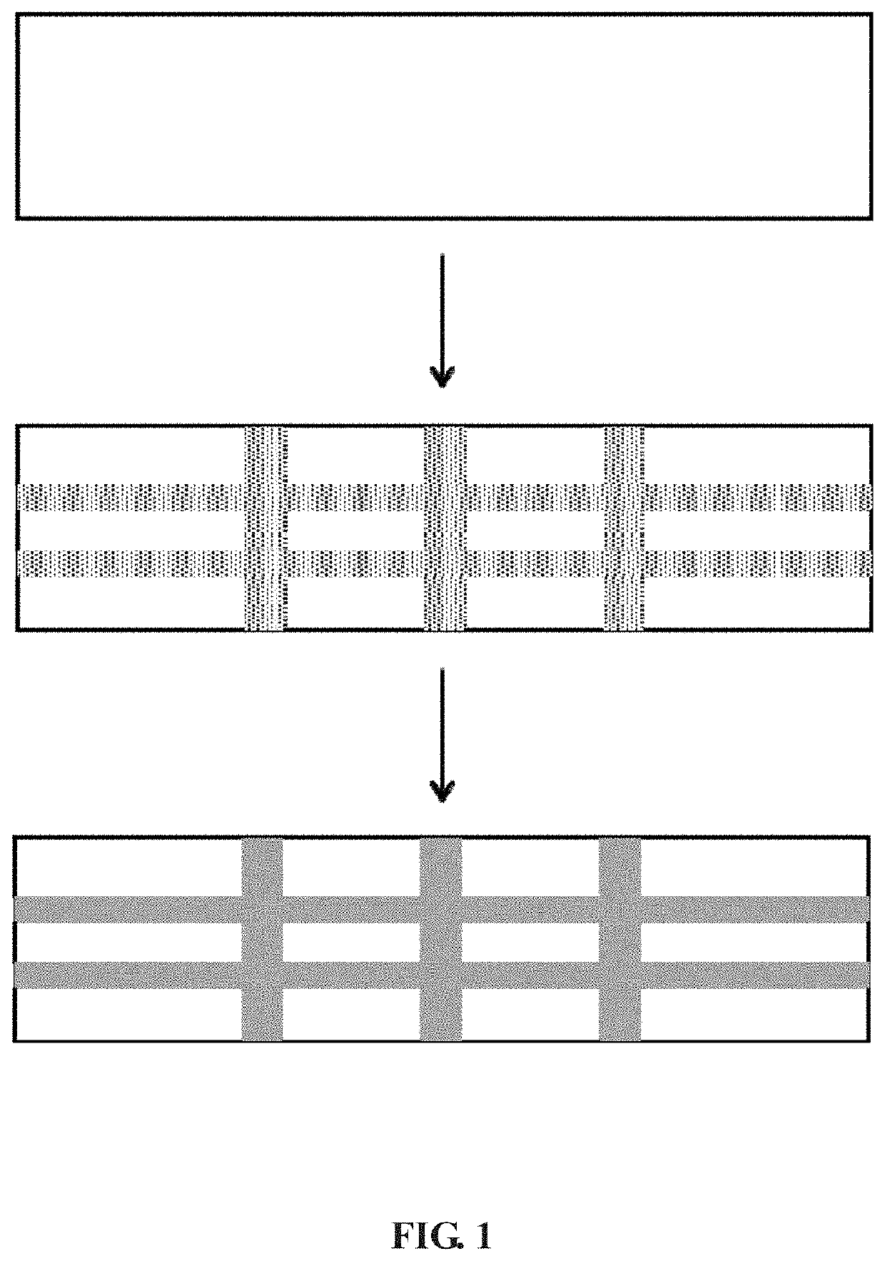
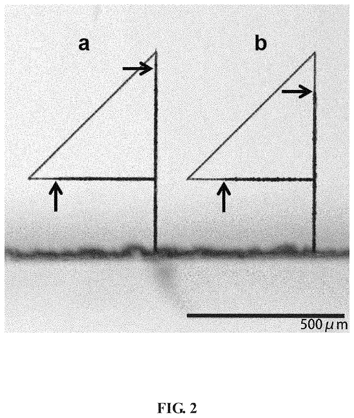
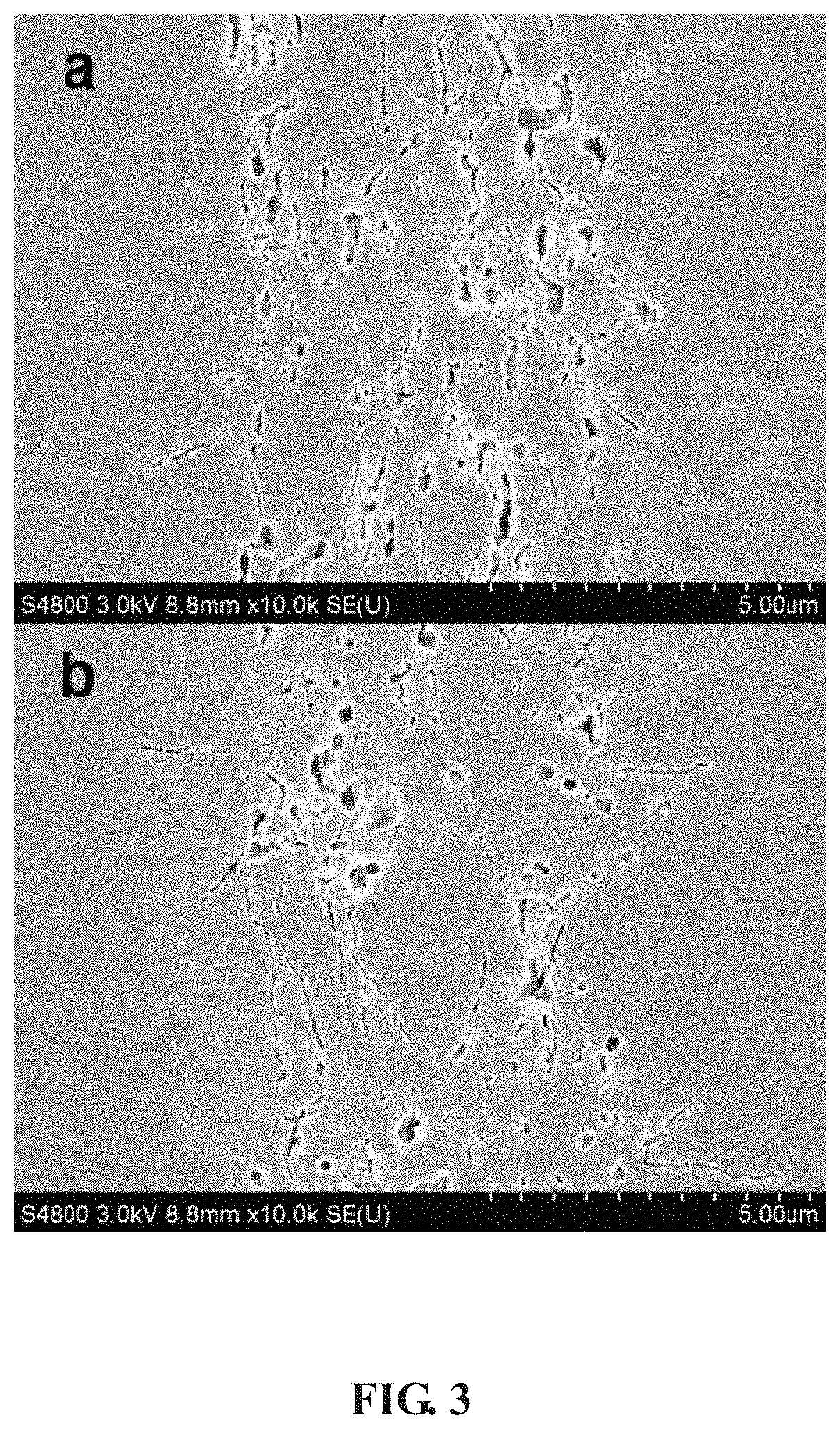
[0025]As shown in FIG. 1, fixing a clean glass sample of fused silica with a size of 20 mm×10 mm×2 mm and polished on six sides on a three-dimensional positioning stage; the laser operating at a center wavelength of 1026 nm, with a repetition rate of 50 kHz and a pulse width of 8 ps; focusing the laser beam at a depth of 300 μm below the surface of the glass substrate using a microscope objective with a numerical aperture of 0.45 (transmission rate is ˜30% for the beam). To evaluate the effect of polarization on the etch rate, two different polarization states of the output laser beam are used to directly write the patterns: linear polarization with orientation perpendicular to the direct writing direction (marked with “a” in FIG. 2 and FIG. 3), circular polarization which is produced by employing a quarter-wave plate prior to the objective ...

embodiment 2

[0028]In the second embodiment of the present invention, the method comprises the following steps:

[0029]Step 1: Picosecond Laser Beam Irradiation

[0030]As shown in FIG. 1, fixing a clean glass sample of fused silica with a size of 5 mm×5 mm×5 mm and polished on six sides on a three-dimensional positioning stage; the laser operating at a center wavelength of 1026 nm, with a repetition rate of 50 kHz and a pulse width of 8 ps; focusing the light beam via a microscope objective with a numerical aperture of 0.30 (transmission rate is ˜50% for the beam), placing a quarter-wave plate before the microscope objective to generate a circularly polarized beam, writing a six-sided microchannel multilayer grid pattern inside the glass sample. The pulse energy prior to the objective and the scanning speed are 9 μJ and 0.5 mm / s, respectively.

[0031]Step 2: Selective Chemical Etching

[0032]Placing the glass sample irradiated by picosecond laser beam in a 10 mol / L potassium hydroxide solution (85 ° C.)...

embodiment 3

[0033]In the third embodiment of the present invention, the method comprises the following steps:

[0034]Step 1: Picosecond Laser Beam Irradiation

[0035]Fixing a clean glass sample of fused silica with a size of 5 mm×5 mm×1 mm and polished on six sides on a three-dimensional positioning stage; the laser operating at a center wavelength of 1026 nm, with a repetition rate of 50 kHz and a pulse width of 10 ps; focusing the light beam via a microscope objective with a numerical aperture of 0.45 (transmission rate is ˜30% for the beam), placing a quarter-wave plate before the microscope objective to generate a circularly polarized beam, writing a three-dimensional microcoil pattern with a coil diameter of 200 μm and a period of 150 μm inside the glass sample. The pulse energy prior to the objective and the scanning speed are 4 μJ and 0.5 mm / s, respectively.

[0036]Step 2: Selective Chemical Etching

[0037]Placing the glass sample irradiated by picosecond laser beam in a 10 mol / L potassium hydro...


PUM

PropertyMeasurementUnit
sizeaaaaaaaaaa
depthaaaaaaaaaa
etch ratesaaaaaaaaaa

Abstract

Method of fabricating a microfluidic device by means of inducing internal cracks in fused silica employing a picosecond laser beam, firstly utilizing irradiation of a focused temporally controlled picosecond laser beam in fused silica to generate a spatially selective modification region including randomly oriented nanocracks, then employing chemical etching to remove the irradiated area and obtain a hollow and connected three-dimensional microstructure, thereby achieving three-dimensional fabrication of microchannel structures inside the fused silica. The method can realize polarization insensitive three-dimensional uniform etching by regulating the pulse width of the picosecond laser beam, and has high chemical etch rate and selectivity, applicable for fabrication of large-sized three-dimensional microfluidic systems, high-precision 3D glass printing, etc.

Description

CROSS-REFERENCE TO RELATED APPLICATION[0001]The subject application claims priority on Chinese patent application CN201811539810.9 filed on Dec. 17, 2018 in China. The contents and subject matter of the Chinese priority application is incorporated herein by reference.FIELD OF INVENTION[0002]The present invention relates to method for fabricating a three-dimensional microchannel and microfluidic device, particularly, a method for fabricating a microfluidic device in fused silica using picosecond laser irradiation, which is applicable for fabrication of large-sized glass-based microfluidic systems, high-precision 3D glass printing, etc.BACKGROUND OF INVENTION[0003]Microfluidic chip technology is a revolutionary technology that has shown important applications in chemical synthesis and analysis, biopharmaceuticals, medical diagnostics, photonics, etc. A microchannel is the core unit of a microfluidic chip, and its high performance and multi-function fabrication technology are of great ...

Claims


Application Information

Patent Timeline
Patent Type & Authority Applications(United States)
IPC IPC(8): B23K26/0622B81C1/00B01L3/00B23K26/064
CPCB23K26/064B23K26/0624B01L3/502707B81C1/00539B01L2300/0874B23K26/53B23K26/55B23K26/0006B23K2103/54B23K26/08C03C15/00C03C3/06C03C23/0025B81C1/00119
Inventor CHENG, YAXU, JIANLI, XIAOLONG
Owner EAST CHINA NORMAL UNIV
Why Eureka
Try Eureka