Anti-ejection apparatus for wafer units
a technology of anti-ejection apparatus and wafer unit, which is applied in the direction of electrical apparatus, basic electric elements, and semiconductor devices, can solve the problems of high cost and achieve the effect of high cos
- Summary
- Abstract
- Description
- Claims
- Application Information
AI Technical Summary
Benefits of technology
Problems solved by technology
Method used
Image
Examples
embodiment
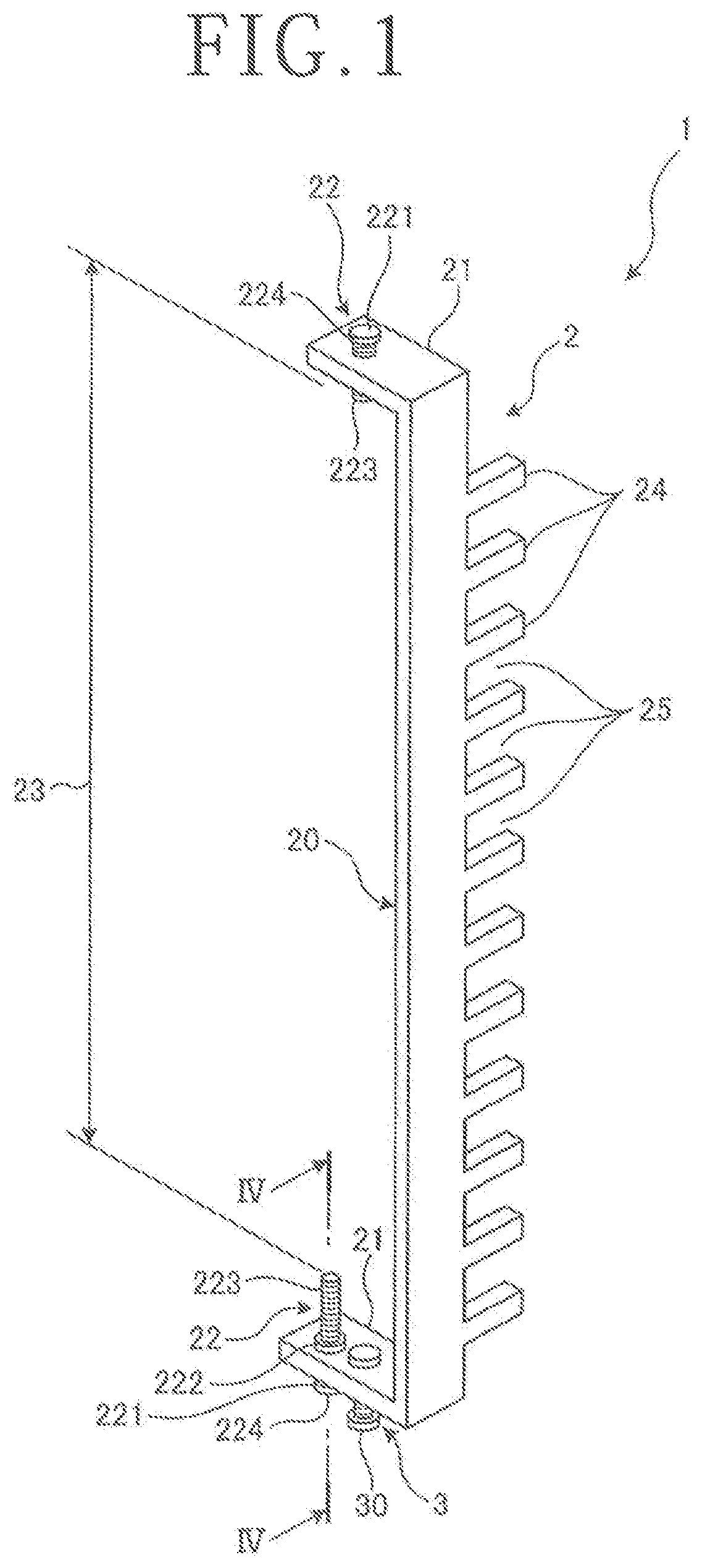
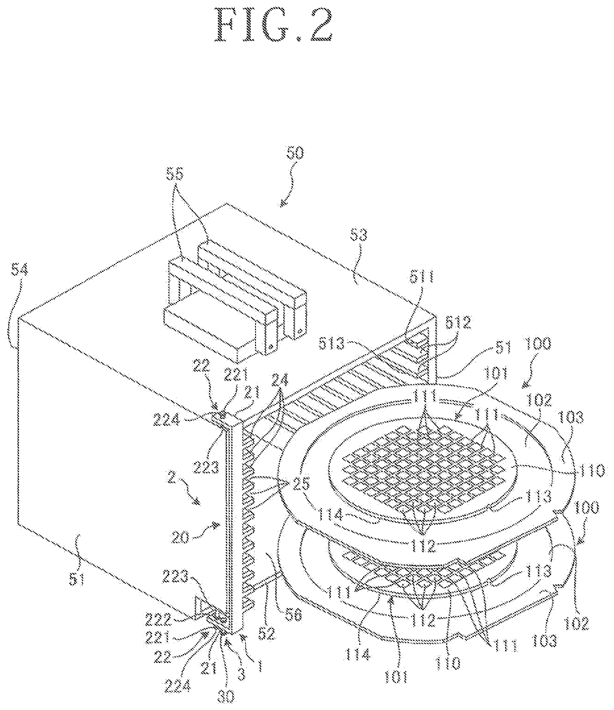
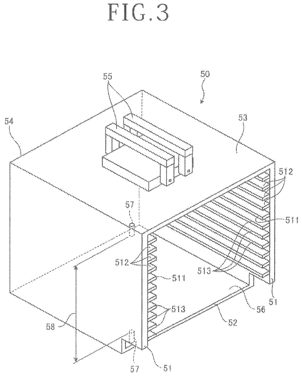
[0019]An anti-ejection apparatus according to the embodiment of the present invention for wafer units will be described based on the relevant figures of the drawings. FIG. 1 is a perspective view depicting a configuration example of an anti-ejection apparatus according to an embodiment for wafer units. FIG. 2 is a perspective view depicting the anti-ejection apparatus of FIG. 1 together with a cassette to which the anti-ejection apparatus is attached. FIG. 3 is a perspective view of the cassette depicted in FIG. 2. FIG. 4 is a cross-sectional view taken along line IV-IV in FIG. 1.
[0020]The anti-ejection apparatus of FIG. 1 according to the embodiment for the wafer units (hereinafter simply referred to as “the anti-ejection apparatus”) is used in attachment to a cassette 50 as depicted in FIG. 2. The cassette 50 is a container that as depicted in FIG. 2, can contain a plurality of wafer units 100 of ring-shaped frames 103 and wafers 101 integrated together via adhesive tapes 102, res...
first modification
[0047]An anti-ejection apparatus according to a first modification of the embodiment of the present invention for wafer units will be described based on the relevant figure of the drawings. FIG. 9 is a cross-sectional view of a lower bar mounting fixture of the anti-ejection apparatus according to the first modification of the embodiment for wafer units. In FIG. 9, like elements as in the embodiment are identified by like reference numerals, and their description is omitted herein.
[0048]The anti-ejection apparatus 1-1 according to the first modification for the wafer units (hereinafter simply referred to as “the anti-ejection apparatus”) has the same configuration as the anti-ejection apparatus 1 according to the embodiment except for a difference in the configuration of the bar attachment fixtures 22 that the recesses 57 are not included. As depicted in FIG. 9, a lower bar attachment fixture 22-1 of the anti-ejection apparatus 1-1 is fixedly secured between the lower surface of the...
second modification
[0050]An anti-ejection apparatus according to a second modification of the embodiment of the present invention for wafer units will be described based on the relevant figure of the drawings. FIG. 10 is a cross-sectional view of a guide pin of the anti-ejection apparatus according to the second modification of the embodiment for the wafer units. In FIG. 10, like elements as in the embodiment are identified by like reference numerals, and their description is omitted herein.
[0051]The anti-ejection apparatus 1-2 according to the second modification for the wafer units (hereinafter simply referred to as “the anti-ejection apparatus”) has the same configuration as the anti-ejection apparatus 1 according to the embodiment except for a difference in the configuration for attachment of a guide pin 3-2 to the lower attachment part 21. As depicted in FIG. 10, the guide pin 3-2 of the anti-ejection apparatus 1-2 includes a cylindrical threaded portion 31 with a thread formed on an outer periph...
PUM
 Abstract
Description
Claims
Application Information


