Display panel and manufacturing method thereof

a technology of display panel and manufacturing method, applied in the field of display panel, can solve problems such as screen tearing

Active Publication Date: 2022-02-15
WUHAN CHINA STAR OPTOELECTRONICS SEMICON DISPLAY TECH CO LTD
View PDF16 Cites 0 Cited by
  • Summary
  • Abstract
  • Description
  • Claims
  • Application Information

AI Technical Summary

Benefits of technology

[0004]An embodiment of the present disclosure provides a display panel and a manufacturing method thereof to solve the problem of screen tearing which is easily caused during an aging test process in the display panel.
[0028]The beneficial effect of the present disclosure is that by disposing the first connecting line in the first single-sided driving area and connecting the first connecting line to the input terminal of the first GOA circuit, and by disposing the second connecting line in the second single-sided driving area and connecting the second connecting line to the input terminal of the second GOA circuit, the first connecting line and the second connecting line are connected when a lighting signal is respectively input to the input terminal of the first GOA circuit and the input terminal of the second GOA circuit, which ensures consistencies of input signals of the GOA circuits at both sides, thereby preventing screen tearing which is caused by single-sided driving when performing an aging test, and improving a yield of the display panel.

Problems solved by technology

This method has a high requirement for bonding accuracy when lighting, which will cause inconsistencies of input signals of the GOA circuits at the both sides if there is a slight offset when an aging test is performed on a display panel, thereby resulting in screen tearing.

Method used


Image

  • Display panel and manufacturing method thereof
  • Display panel and manufacturing method thereof
  • Display panel and manufacturing method thereof

Examples


Embodiment Construction

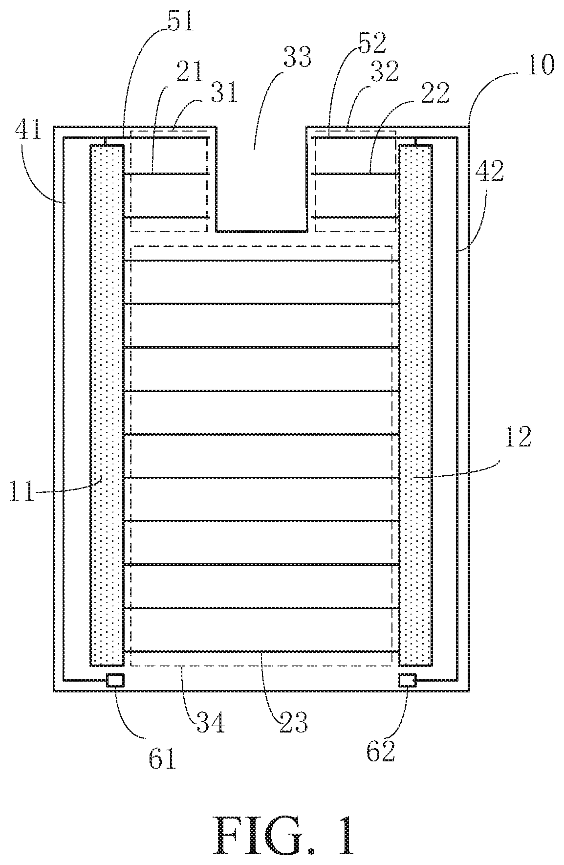
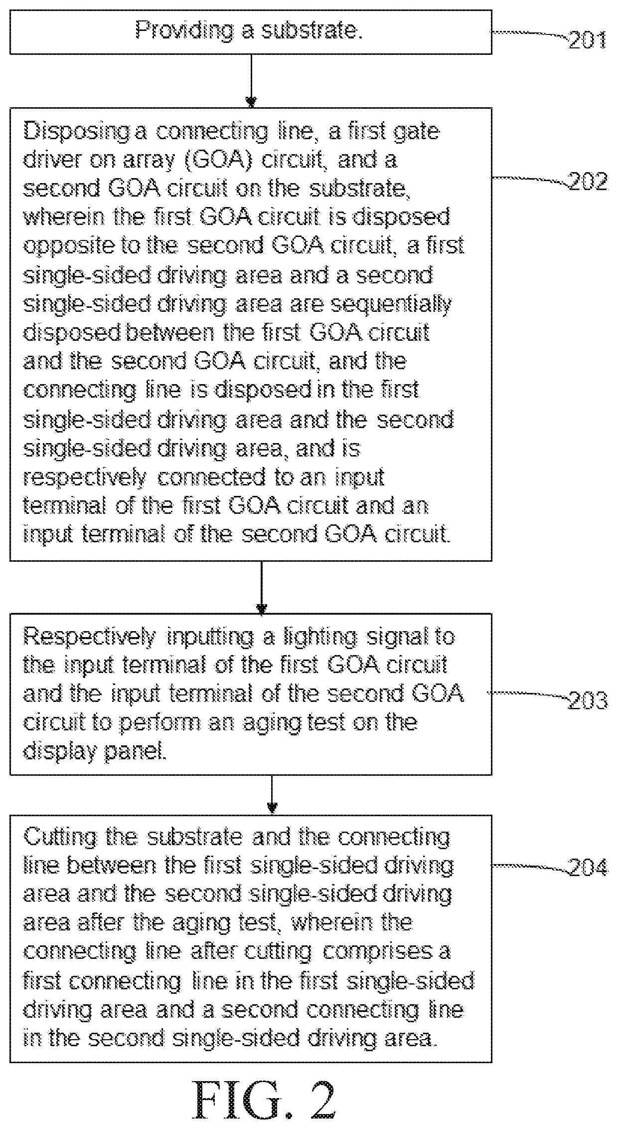
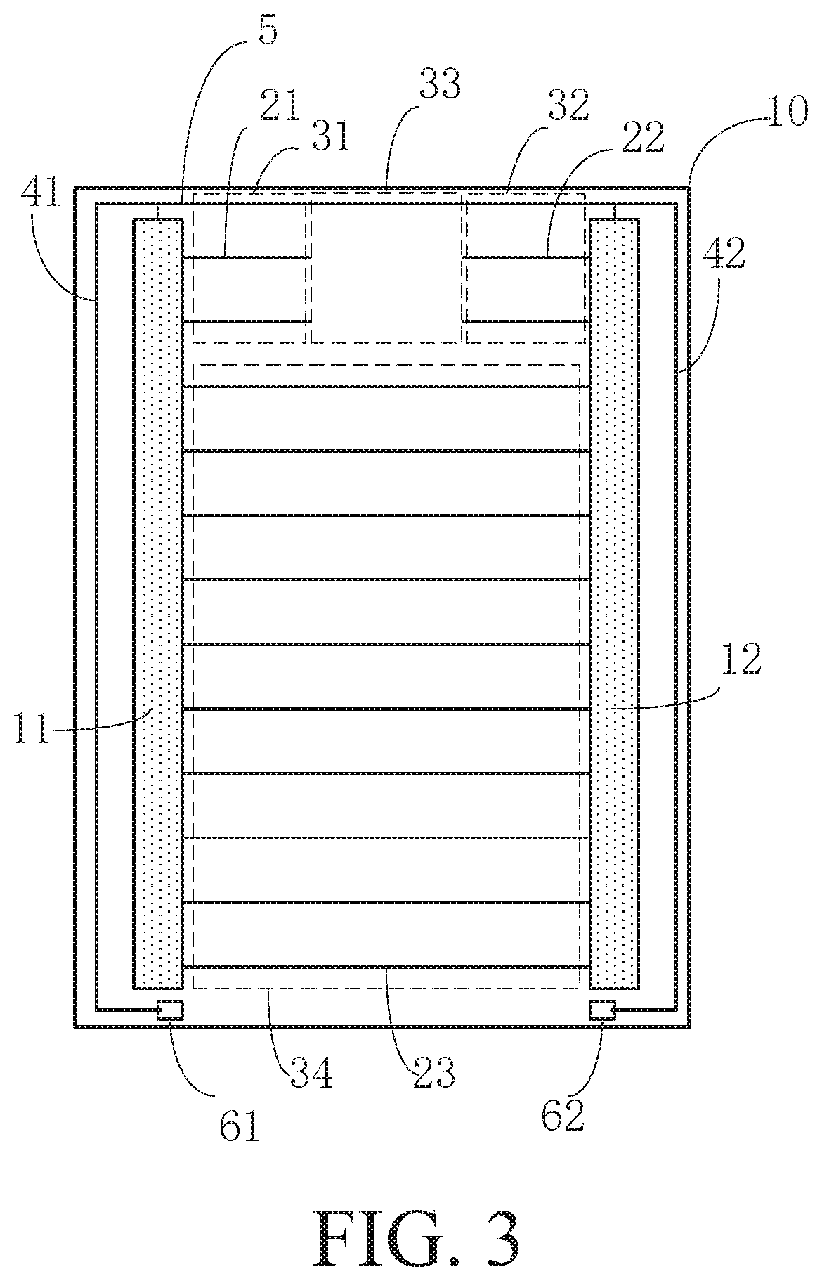
[0033]The specific structures and functional details disclosed herein are merely representative and are for the purpose of describing exemplary embodiments of the present disclosure. In addition, this disclosure can be implemented in many alternative forms, and should not be interpreted as being limited to the embodiments set forth herein.

[0034]In the description of the present disclosure, it should be understood that terms such as “center”, “lateral”, “upper”, “lower”, “left”, “right”, “vertical”, “horizontal”, “top”, “bottom”, “inside”, “outside”, as well as derivative thereof should be construed to refer to the orientation as described or as shown in the drawings under discussion. These relative terms are for convenience of description, do not require that the present disclosure be constructed or operated in a particular orientation, and shall not be construed as causing limitations to the present disclosure. In addition, terms such as “first” and “second” are used herein for pur...


PUM


Abstract

A display panel and a manufacturing method thereof are provided. The display panel includes a substrate, and a first connecting line, a second connecting line, a first GOA circuit, and a second GOA circuit disposed on the substrate. The first GOA circuit is disposed opposite to the second GOA circuit, and a first single-sided driving area and a second single-sided driving area are sequentially disposed between the first GOA circuit and the second GOA circuit. The first connecting line is disposed in the first single-sided driving area and connected to an input terminal of the first GOA circuit, and the second connecting line is disposed in the second single-sided driving area and connected to an input terminal of the second GOA circuit. The present disclosure can prevent screen tearing which is caused by single-sided driving when performing an aging test, and improve a yield of the display panel.

Description

RELATED APPLICATION[0001]This application claims the benefit of priority of Chinese Patent Application No. 202010286146.2 filed on Apr. 13, 2020, the contents of which are incorporated herein by reference in their entirety.FIELD AND BACKGROUND OF THE INVENTION[0002]The present disclosure relates to the field of display panel technologies, and more particularly, to a display panel and a manufacturing method thereof.[0003]In order to improve screen ratio, notch screens (display screens having a notch structure) are getting more popular. However, a presence of the notch structure makes output terminals of gate driver on array (GOA) circuits at both sides of the display screens need to use a single-sided driving method. This method has a high requirement for bonding accuracy when lighting, which will cause inconsistencies of input signals of the GOA circuits at the both sides if there is a slight offset when an aging test is performed on a display panel, thereby resulting in screen tear...

Claims


Application Information

Patent Timeline
Patent Type & Authority Patents(United States)
IPC IPC(8): G09G3/20G01R31/28
CPCG09G3/20G01R31/2849G09G2300/0408G09G2310/0202G09G2310/0267G09F9/30G01R31/2843
Inventor XIONG, RUI
Owner WUHAN CHINA STAR OPTOELECTRONICS SEMICON DISPLAY TECH CO LTD
Why Eureka
Try Eureka