Semiconductor wafer and method for fabrication thereof

a technology of semiconductor and silicon wafer, which is applied in the manufacturing of semiconductor/solid-state devices, basic electric elements, electric devices, etc., can solve the problems of reducing the flatness of the wafer, affecting the chucking and releasing of the wafer, and affecting the chucking effect of the wafer

Inactive Publication Date: 2002-03-05
SHIN-ETSU HANDOTAI CO LTD
View PDF7 Cites 34 Cited by
  • Summary
  • Abstract
  • Description
  • Claims
  • Application Information

AI Technical Summary

Benefits of technology

When the wafer of the present invention is used, there are no grinding striations remaining on the front surface which are formed in the case of the conventional wafer fabricated by conducting lapping of the both surfaces, surface-grinding of the front surface or the both surfaces, double side polishing, and mirror-polishing. Furthermore, when the wafer of the present invention is chucked at the back surface thereof, there are no problems, which may be easily caused in a device process because of too good flatness of the back surface, such as indistinguishability of the front surface from the back surface, necessity of re-adjustment of sensing sensitivity, difficulty of chucking and releasing the wafer, and liabilities in a conveying line such as contamination. Furthermore, the grinding striations on the back surface are never transferred on the front surface in fabrication of the wafer of the present invention. Accordingly, it can be used in a process of highly integrated devices, productivity and yield of a device can be improved, and cost can be significantly reduced.
According to the above-mentioned method comprising the double side lapping step, the single side surface-grinding step, the double side polishing step and the step of subjecting the other surface than the above ground surface to a finishing mirror-polishing, a wafer having high flatness can be easily fabricated at low cost, as compared with the conventional method comprising a double side lapping step, a step of grinding a front surface or both surfaces, a double side polishing step and a mirror-polishing step. Furthermore, a problem of grinding striations remaining on the surface, which is one of disadvantages in the conventional method, can be solved, and a wafer having a front surface comprising a mirror surface without grinding striations and micro roughness and a back surface with desired grinding striations, can be fabricated easily and at low cost.
When the mirror edge polishing (mirror-polishing on chamfered edge) is conducted before or after the double side polishing step, defects such as cracking or breakage of the wafer can be prevented during polishing or in a device process. The mirror edge polishing is more effective, since it is conducted after the peripheral edge portion of the wafer is ground for coarse chamfering before the lapping step in order to prevent cracking or breakage of the wafer or the like during lapping and a surface-grinding.
Thereby, it is possible to remove a mechanical damage layer of the wafer, maintaining flatness achieved by the double side lapping step, and to conduct a polishing step effectively with maintaining high flatness, in cooperation with the following single side grinding. A stock removal of the wafer in the etching treatment can be minimal for removing the mechanical damage layer.
As described above, according to the present invention, a semiconductor wafer having the front surface which is a mirror surface with high flatness and high brightness and without micro roughness and the back surface having appropriate fine grinding striations can be fabricated easily and at low cost. Accordingly, when the wafer is chucked in a device process, the grinding striations on the back surface are never transferred on the front surface of the wafer of the present invention, and it can be used in a process of highly integrated devices, productivity and yield of a device can be improved in a device process, and cost can be significantly reduced.

Problems solved by technology

Furthermore, if it is polished in a considerable amount, the wafer may lose its proper shape, and flatness thereof is degraded.
In the case of the wafer having high flatness wherein both surfaces are subjected to mirror-polishing, flatness on the back surface is too good, which may easily cause problems in a device process, such as indistinguishability of the front surface from the back surface, necessity of re-adjustment of sensing sensitivity, difficulty of chucking and releasing the wafer, and liabilities in a conveying line such as contamination.

Method used


Image

  • Semiconductor wafer and method for fabrication thereof
  • Semiconductor wafer and method for fabrication thereof
  • Semiconductor wafer and method for fabrication thereof

Examples


example

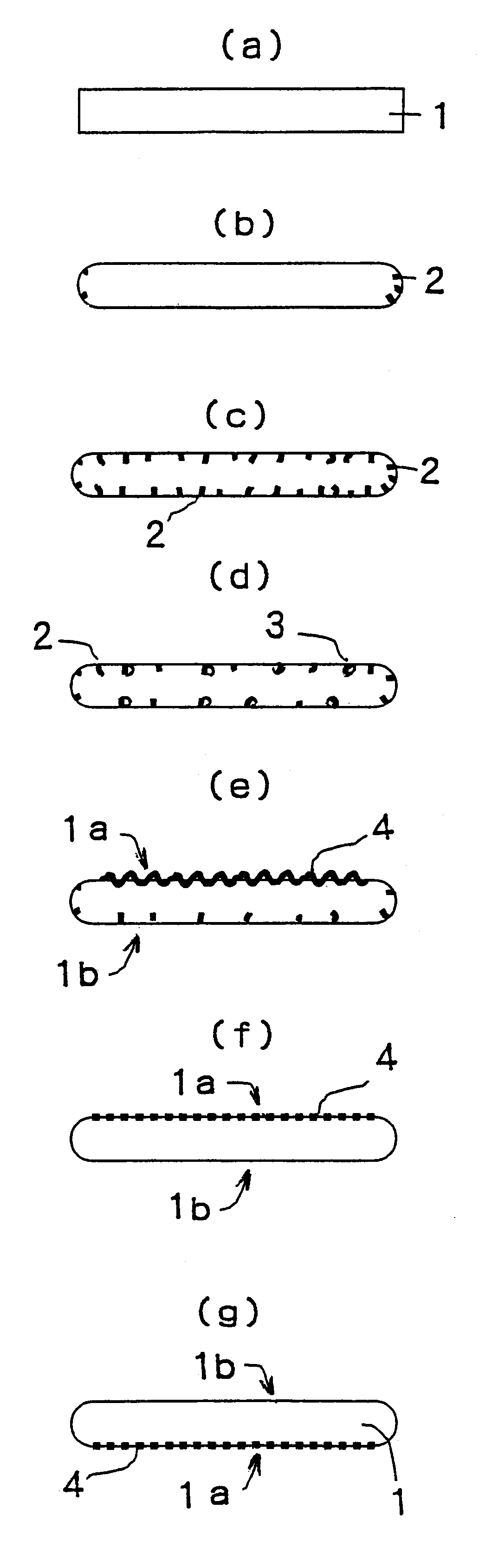
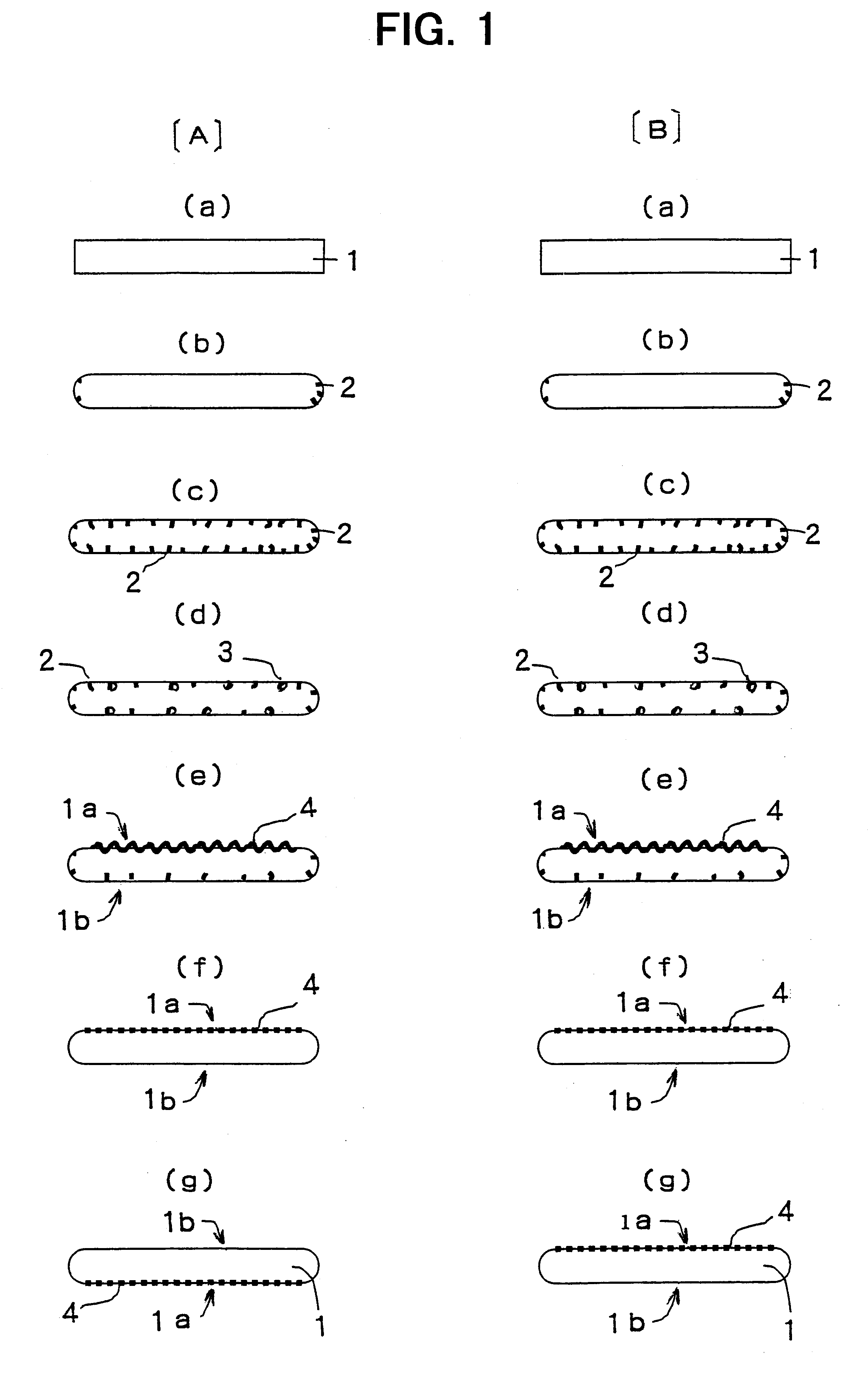
Semiconductor wafers were fabricated from a semiconductor ingot according to the method shown in FIG. 1 [A] (a) to (g). 200 of them were determined as for their quality.

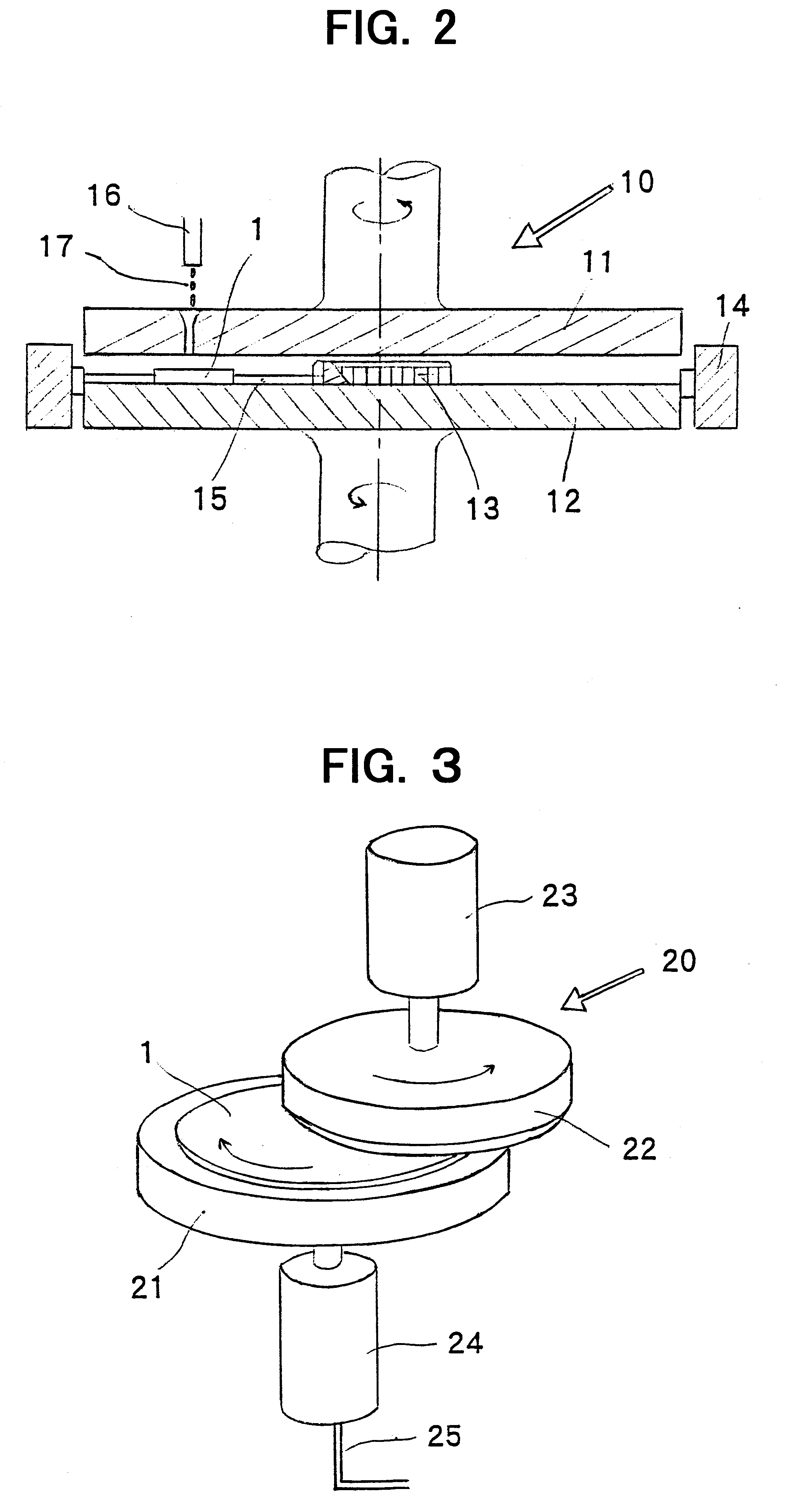
The apparatuses described above, namely, a double side lapping apparatus, a single side grinding apparatus, a double side polishing apparatus, a single side finishing mirror-polishing apparatus or the like were mainly used.

The wafers having a diameter of 300 mm and a thickness of 975 .mu.m were obtained as a starting material by a slicing step, and subjected to lapping, grinding, polishing and the like.

The steps of lapping, grinding and polishing were conducted as follows with varying conditions therefor.

The double side lapping step was conducted varying a stock removal in the range from 80 to 200 .mu.m as a value of those of both surfaces put together.

The etching step was conducted using an alkali solution or acid solution with a sufficient stock removal to remove a mechanical damage layer formed during lapping.

The ...


PUM


Abstract

There is disclosed a semiconductor wafer obtained, at least, by removing a mechanical damage layer by etching both surfaces of the wafer, flattening one of the surfaces by a surface-grinding means, polishing both of the surfaces, and then subjecting a front surface of the wafer to a finishing mirror-polishing when defining the surface subjected to surface-grinding as a back surface of the wafer, and a method for fabricating it. There can be provided a method for fabricating a semiconductor wafer wherein grinding striations which remain on a semiconductor wafer even when double side polishing and finishing mirror-polishing are conducted after a conventional step of surface-grinding of the front surface or the both surfaces, are eliminated to improve quality of the front surface of the wafer, and the back surface having a quality suitable for the device process can be obtained, and a semiconductor wafer obtained thereby.

Description

1. Field of the InventionThe present invention relates to a semiconductor wafer, and especially a method for fabrication of a single crystal silicon wafer.2. Description of the Related ArtGenerally, a conventional method for fabricating a semiconductor wafer comprises a slicing step to obtain wafers of a thin disc shape by slicing a single crystal silicon ingot pulled with a single crystal pulling apparatus; a coarse chamfering step to chamfer a peripheral edge portion of the sliced wafer in order to prevent cracking or breakage of the wafer; a lapping step to flatten both of the front surface and the back surface of the chamfered wafer; a cleaning or etching step to remove a remaining mechanical damage layer formed by the chamfering step and lapping step; and a mirror-polishing step to mirror-polish the front surface of the etched wafer. As shown in FIG. 1 [B], adding to these steps, there can be conducted by combination of a step of surface-grinding the front surface or the both s...

Claims


Application Information

Patent Timeline
Patent Type & Authority Patents(United States)
IPC IPC(8): H01L21/02H01L21/304H01L21/306
CPCH01L21/02008H01L21/304
Inventor KISHIMOTO, JUN
Owner SHIN-ETSU HANDOTAI CO LTD
Why Eureka
Try Eureka