De-jaggy processing system and method for OLED display with curved space
a processing system and oled display technology, applied in the field of signal processing, can solve the problems of straight line aliasing (or distortion) artifacts of the oled display, and achieve the effect of reducing or removing jaggy patterns
- Summary
- Abstract
- Description
- Claims
- Application Information
AI Technical Summary
Benefits of technology
Problems solved by technology
Method used
Image

Examples
first embodiment
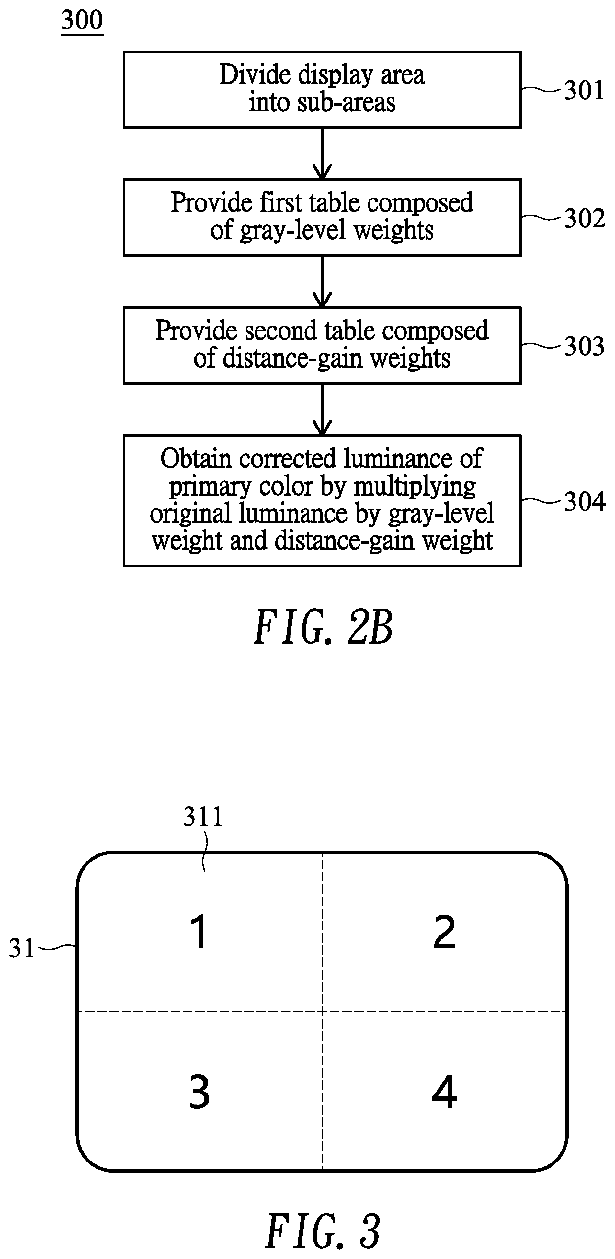
[0024]FIG. 2B shows a flow diagram illustrating a de-jaggy processing method 300 adaptable to an organic light-emitting diode (OLED) display to remove or reduce jaggy patterns at curved bezel of the OLED display according to the present invention. Although the OLED display is demonstrated, it is appreciated that the embodiment may be adapted to other displays as well.
[0025]In step 301, a display area of the OLED display is divided into a plurality of sub-areas. FIG. 3 shows an exemplary display area 31 that is divided into four sub-areas (or quadrants) 311, for example, “1,”“2,”“3” and “4.”
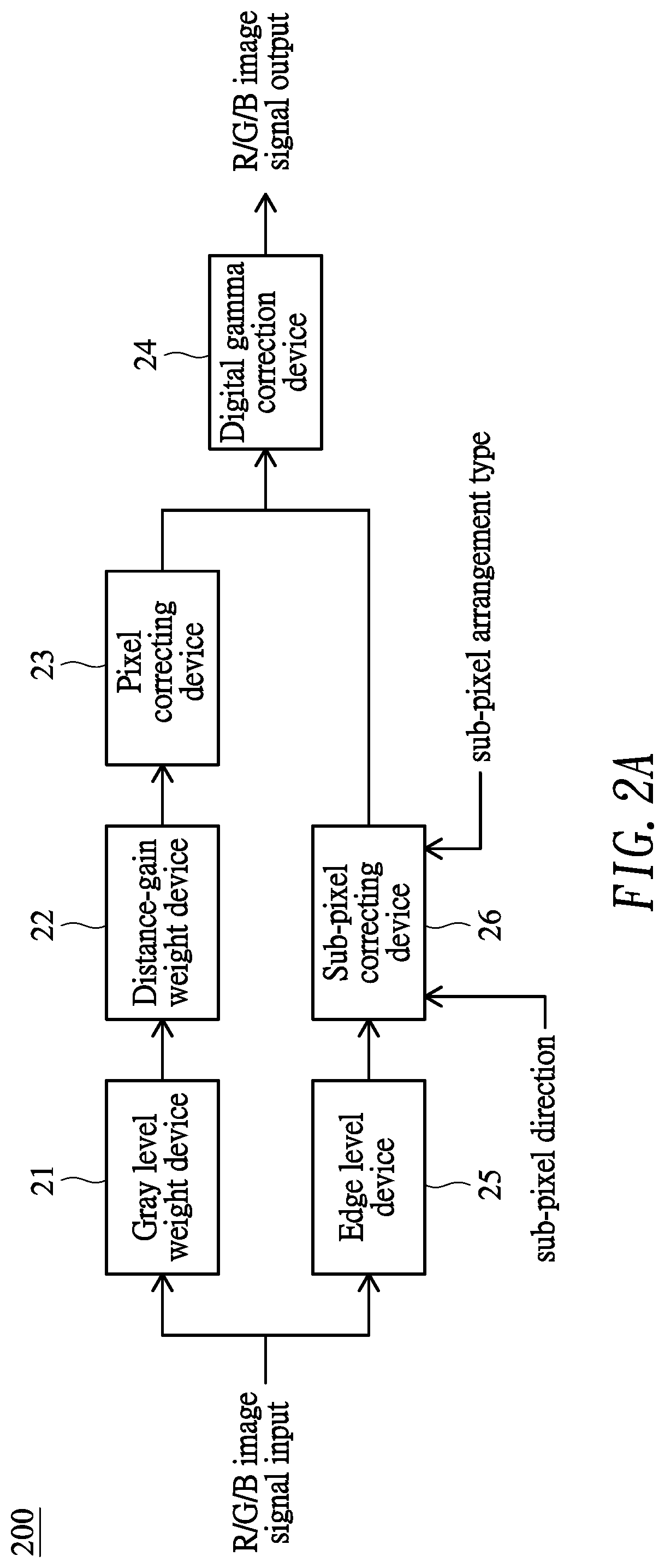
[0026]In step 302, for each sub-area 311, a first table (e.g., lookup table or LUT) composed of gray-level weights for each primary color (red, green or blue) is provided by a gray-level weight device (FIG. 2A). The gray-level weights are associated with corresponding (original) luminances of the primary color. FIG. 4 shows exemplary first tables for sub-areas 311 (e.g., “1,”“2,”“3” and “4”), resp...
second embodiment
[0030]FIG. 6 shows a flow diagram illustrating a de-jaggy processing method 600 adaptable to an organic light-emitting diode (OLED) display to remove or reduce aliasing artifacts along straight lines (e.g., verticals or horizontals) or diagonals of the OLED display according to the present invention. Although the OLED display is demonstrated, it is appreciated that the embodiment may be adapted to other displays as well.
[0031]In step 61, luminance differences (or edge levels) between a current sub-pixel and neighboring sub-pixels are determined by an edge level device 25 (FIG. 2A). FIG. 7 exemplifies a current sub-pixel C and neighboring subpixels (i.e., an upper-left sub-pixel UL, an upper sub-pixel U, an upper-right sub-pixel UR, a left sub-pixel L, a right sub-pixel R, a lower-left sub-pixel DL, a lower sub-pixel D and a lower-right sub-pixel DR). The luminance differences (or edge levels or Ed) of different directions for color red may be expressed as follows:
EdU_R=(R(x,y)−R(x,y...
PUM
| Property | Measurement | Unit |
|---|---|---|
| gray-level weights | aaaaa | aaaaa |
| distance- | aaaaa | aaaaa |
| weights | aaaaa | aaaaa |
Abstract
Description
Claims
Application Information