Touch panel and manufacturing method thereof

a technology of touch panel and manufacturing method, applied in the field of touch panel, can solve the problems of insufficient flexibility, difficult use of metal oxide film, and difficulty in patterned metal oxide film, and achieve the effect of high manufacturing efficiency and process advantages

Active Publication Date: 2022-06-07
TPK ADVANCED SOLUTIONS
View PDF10 Cites 0 Cited by
  • Summary
  • Abstract
  • Description
  • Claims
  • Application Information

AI Technical Summary

Benefits of technology

[0007]According to some embodiments of the present disclosure, a method of manufacturing a touch panel for addressing the foregoing issues is provided. The method has high manufacturing efficiency and process advantages in an application in fine circuits of narrow bezel products.

Problems solved by technology

However, certain characteristics of these metal oxide films have made using these metal oxide films challenging, such as insufficient flexibility.
In some cases, patterned metal oxide films may also be problematic because the patterned metal oxide films are easily observed by users.
However, when using nanowires for manufacturing touch electrodes, there are many problems to be solved in the process and structure of nanowires and metal leads in the peripheral region.
For example, laser processing is used in the traditional process to produce patterns, but laser equipment is costly.
Due to the trend toward narrow bezels and thinning substrates, the control on laser equipment mechanism must be precise, otherwise, it is disadvantageous to mass production of narrow bezel products that require fine circuits.
Also, when a substrate is irradiated with laser, the problem of point-like damage on the substrate may easily occur.

Method used


Image

  • Touch panel and manufacturing method thereof
  • Touch panel and manufacturing method thereof
  • Touch panel and manufacturing method thereof

Examples


Embodiment Construction

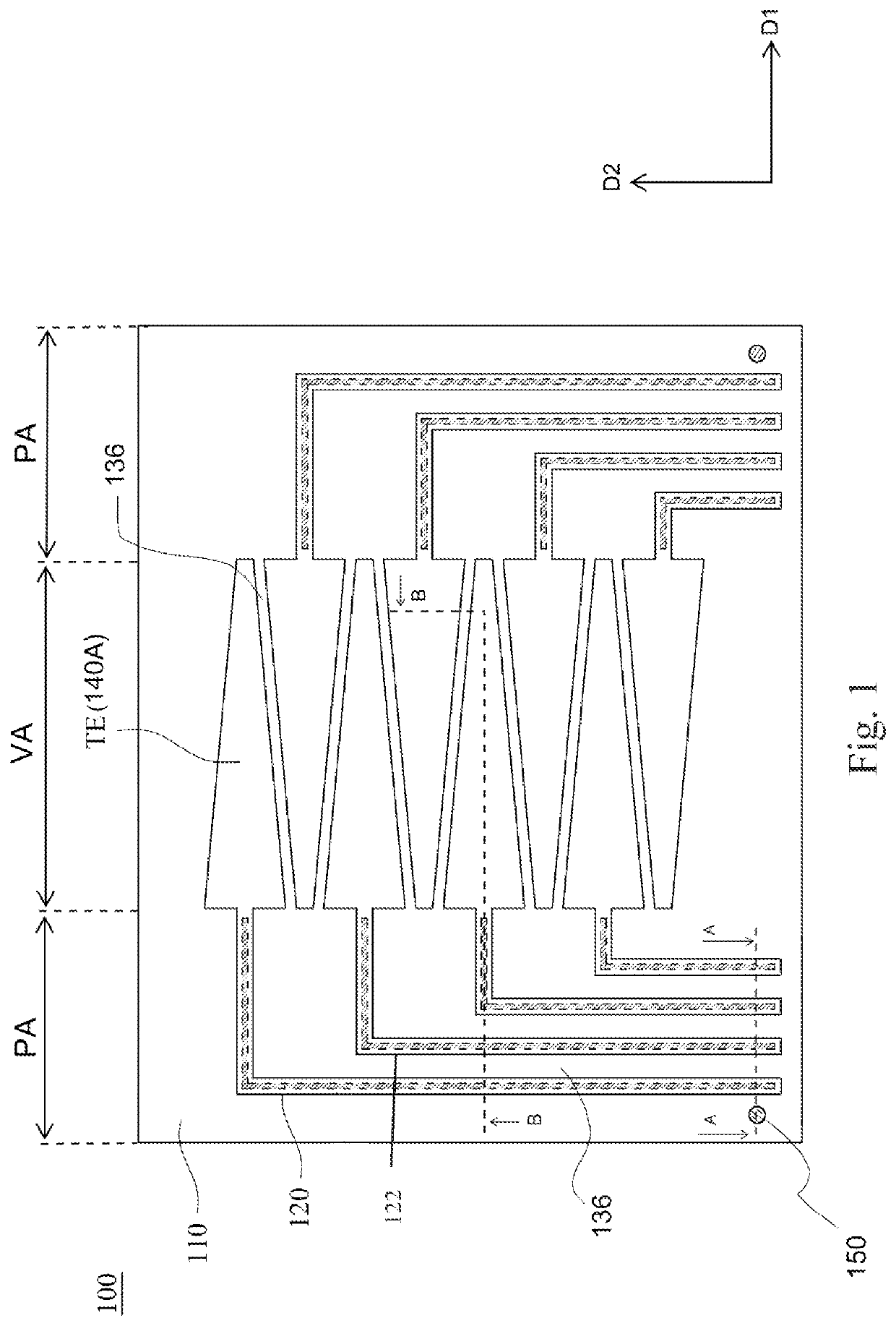
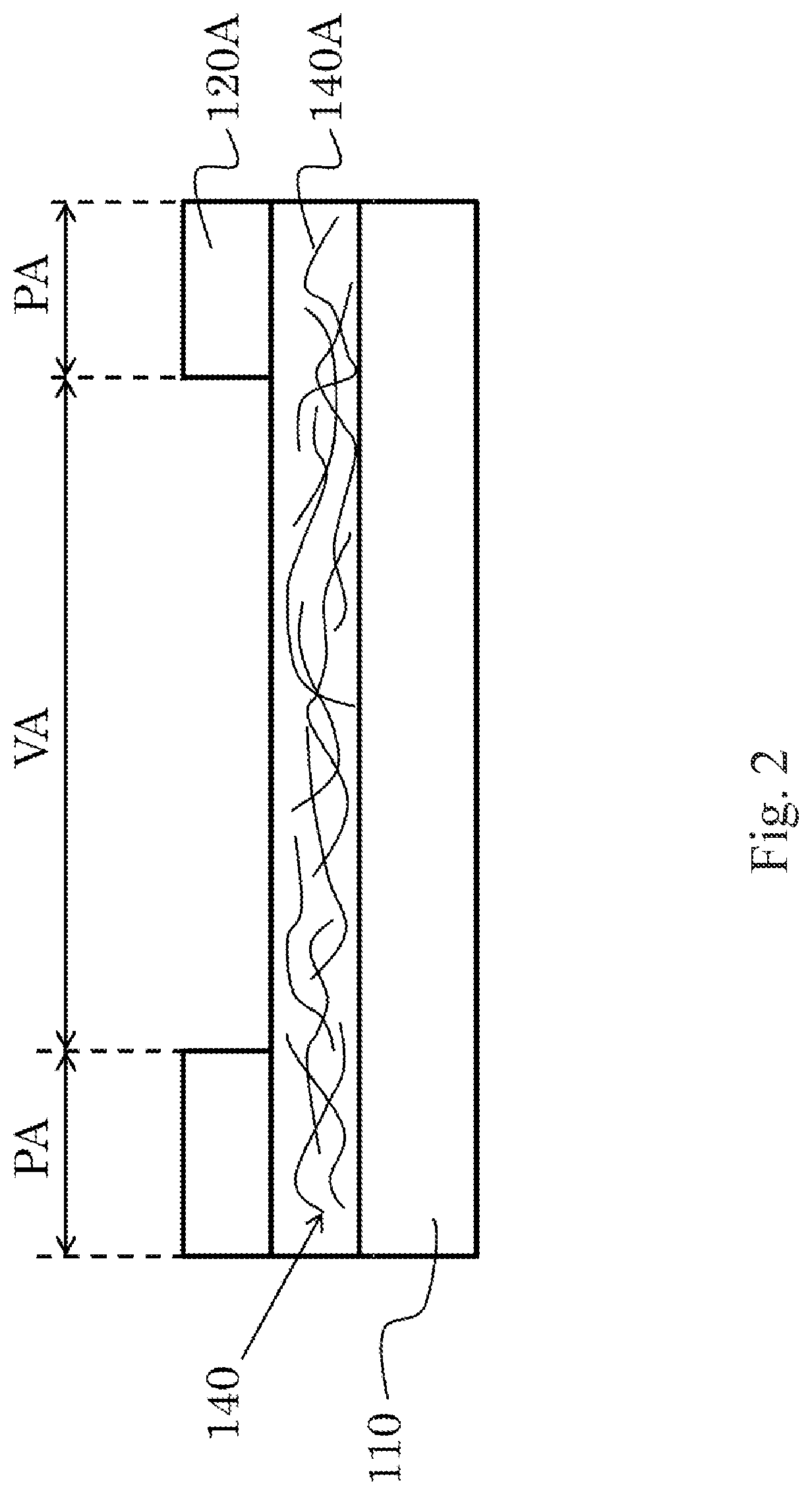
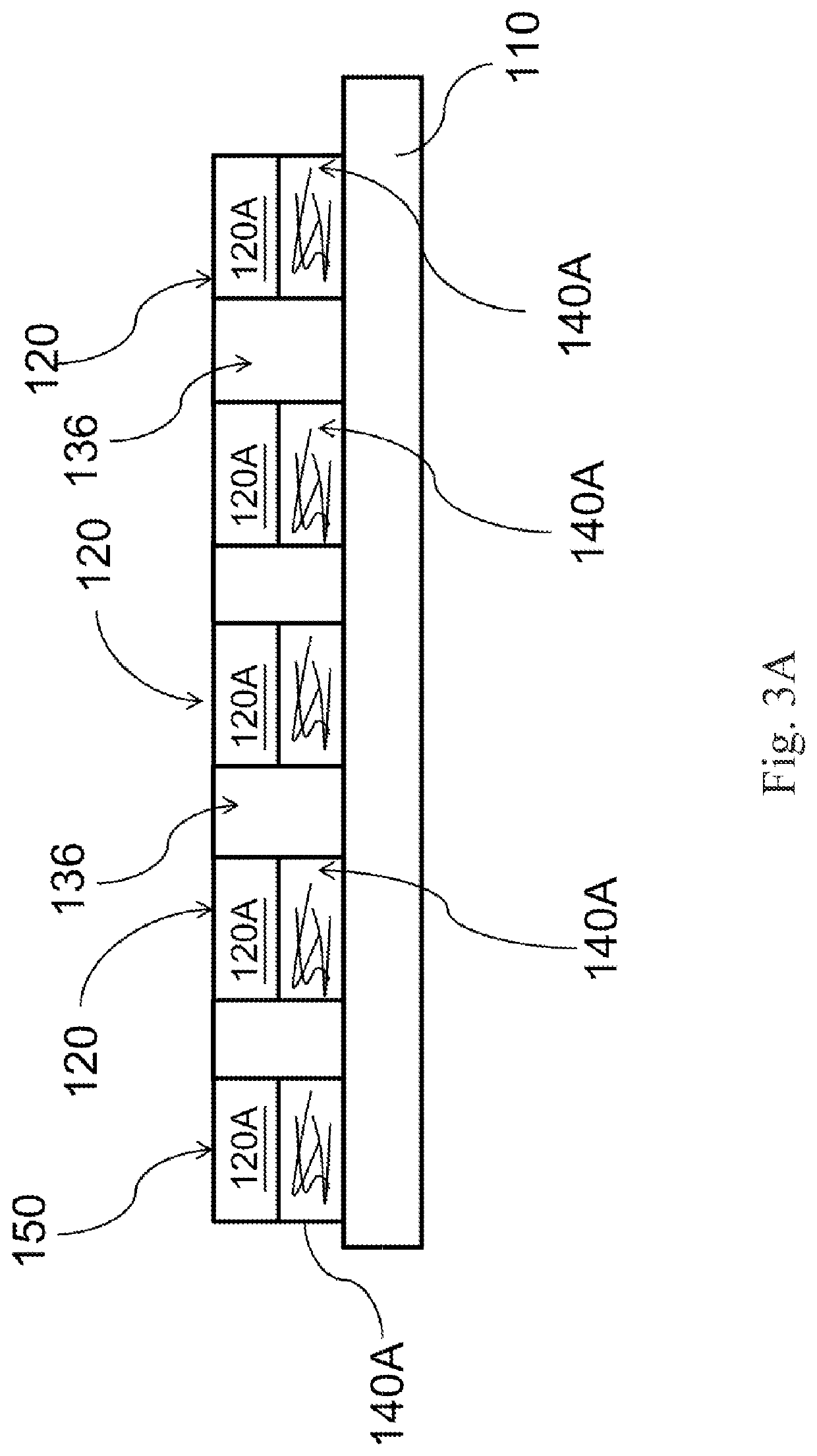
[0035]The following embodiments are disclosed with accompanying diagrams for detailed description. For illustration clarity, many details of practice are explained in the following descriptions. However, it should be understood that these details of practice do not intend to limit the present disclosure. That is, these details of practice are not necessary in parts of embodiments of the present disclosure. Furthermore, for simplifying the drawings, some of the conventional structures and elements are shown with schematic illustrations.

[0036]As used herein, “around”, “about”, or “approximately” shall generally mean within 20 percent, preferably within 10 percent, and more preferably within 5 percent of a given value or range. Numerical quantities given herein are approximate, meaning that the term “around”, “about”, or “approximately” can be inferred if not expressly stated. In addition, it is noted that the terms “pattern”, “image”, and “configuration” used in the present disclosure...


PUM

PropertyMeasurementUnit
diameteraaaaaaaaaa
diameteraaaaaaaaaa
diameteraaaaaaaaaa

Abstract

A touch panel has a substrate having a display region and a peripheral region, a touch sensing electrode disposed in the display region of the substrate, and a peripheral circuit disposed in the peripheral region of the substrate. The touch sensing electrode is electrically connected to the peripheral circuit, and the touch sensing electrode layer includes a first portion of a patterned metal nanowire layer. The peripheral circuit includes a patterned conductive layer and a second portion of the metal nanowire layer. At least a non-conductive material of the conductive layer is between the peripheral circuit and a second peripheral circuit.

Description

CROSS-REFERENCE TO RELATED APPLICATION[0001]This application claims priority to China Application Serial Number 201911413766.1, filed Dec. 31, 2019, which is herein incorporated by reference.BACKGROUNDField of Disclosure[0002]The present disclosure relates to a touch panel and a manufacturing method thereof.Description of Related Art[0003]Since transparent conductors have both light transmissivity and proper conductivity, they can be applied to display panel or touch panel related devices. Generally speaking, transparent conductors can be various metal oxides, such as indium tin oxide (ITO), indium zinc oxide (IZO), cadmium tin oxide (CTO), or aluminum-doped zinc oxide (AZO). However, certain characteristics of these metal oxide films have made using these metal oxide films challenging, such as insufficient flexibility. In some cases, patterned metal oxide films may also be problematic because the patterned metal oxide films are easily observed by users. Therefore, a variety of tran...

Claims


Application Information

Patent Timeline
Patent Type & Authority Patents(United States)
IPC IPC(8): G06F3/044G06F3/041
CPCG06F3/0443G06F3/0412G06F2203/04103G06F3/044G06F3/04164
Inventor WU, SHAN-YUCHEN, CHIH-MIN
Owner TPK ADVANCED SOLUTIONS
Why Eureka
Try Eureka