Package structure and manufacturing method thereof

Active Publication Date: 2022-08-09
WISTRON NEWEB
View PDF5 Cites 0 Cited by
  • Summary
  • Abstract
  • Description
  • Claims
  • Application Information

AI Technical Summary

Benefits of technology

The present patent provides a package structure and manufacturing method that can selectively mold packaging components on a substrate. This is achieved by creating a substrate with a molding area and a non-molding area, where components can be placed on the molding area. This method allows for efficient use of substrate space and simplifies the manufacturing process.

Problems solved by technology

In related art, when packaging semiconductor components or systems, for the sake of the reliability of contact points of solder balls, expensive precision molds are required to be used in a molding process.
Therefore, such selective molding requirement often results in increased mold cost, thereby increasing the overall cost of the module.

Method used


Image

  • Package structure and manufacturing method thereof
  • Package structure and manufacturing method thereof
  • Package structure and manufacturing method thereof

Examples


first embodiment

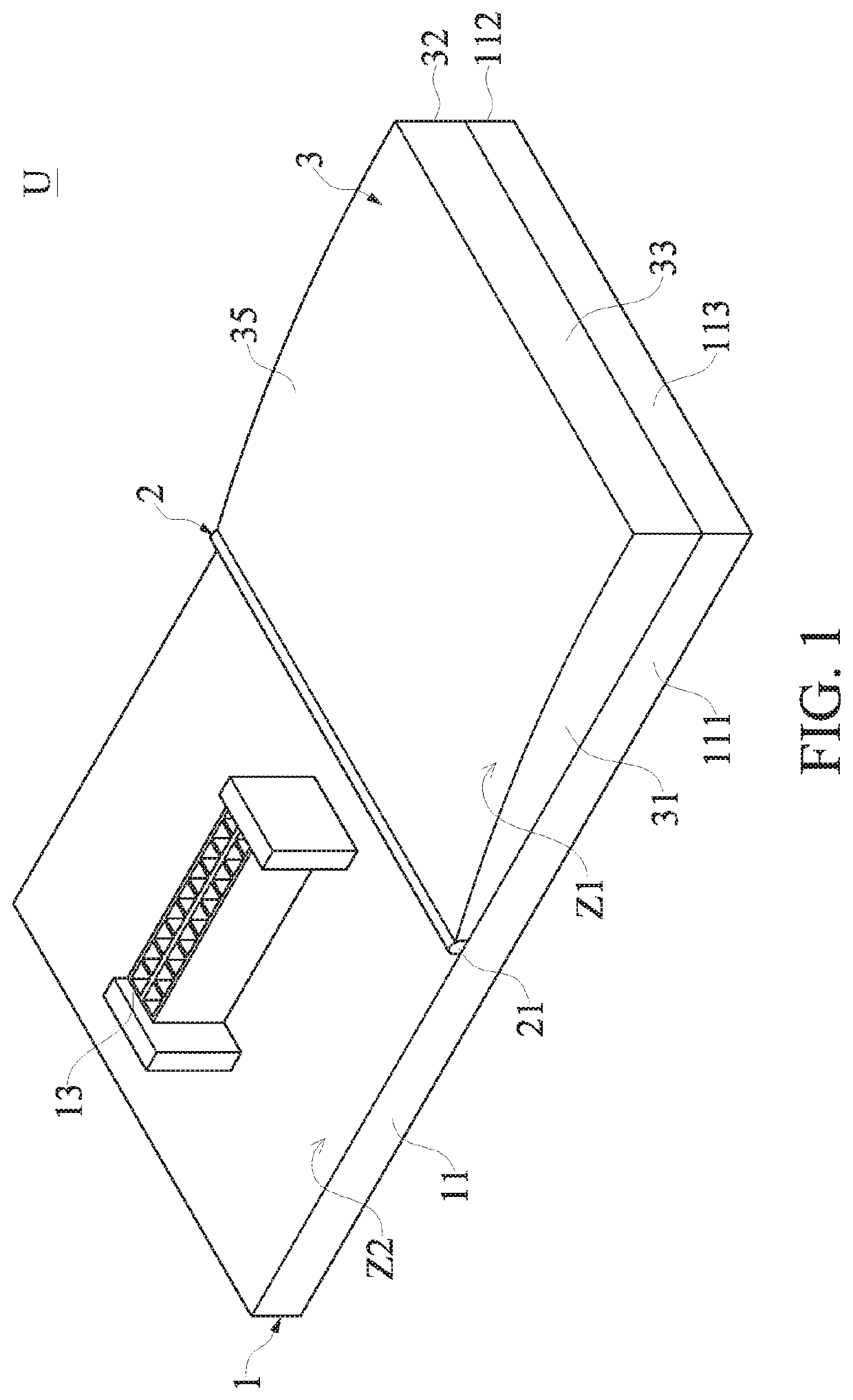
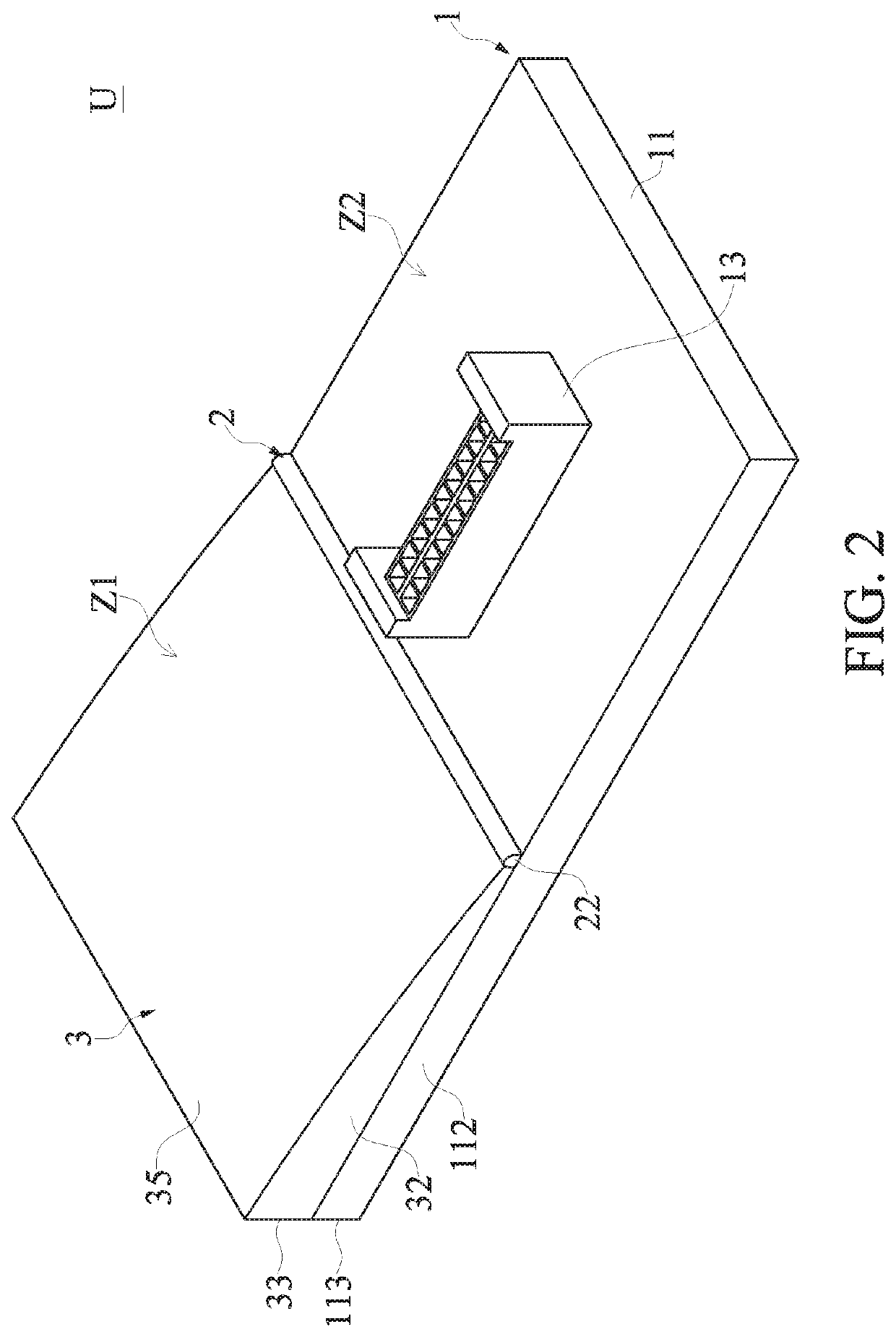
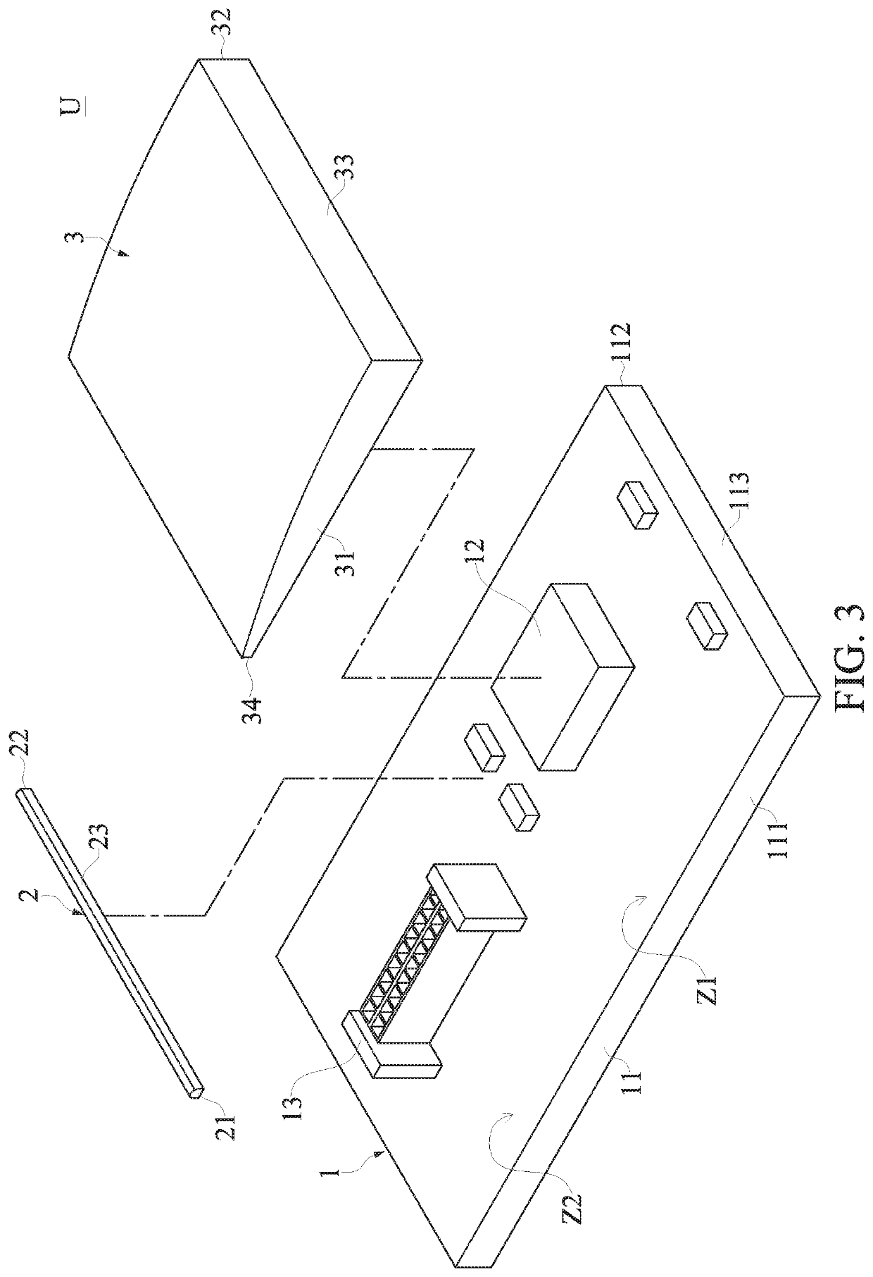
[0033]Firstly, reference is made to FIG. 1, FIG. 2 and FIG. 3, which are a perspective view, an another perspective view and an exploded view of a package structure according to a first embodiment of the present disclosure. The present disclosure provides a package structure U and a manufacturing method thereof. The overall structure of the package structure U will be introduced in the first embodiment, and the manufacturing method of the package structure U will be described in a subsequent embodiment. In addition, it should be noted that, in certain embodiments, the package structure and the manufacturing method thereof provided in the present disclosure can be used for packaging semiconductor components, chips or circuitry. However, the present disclosure is not intended to be limited thereby.

[0034]Subsequently, the package structure U can include a circuit board 1, a barrier structure 2 and a molding layer 3. The circuit board 1 can include a substrate 11 and a component 12 disp...

second embodiment

[0042]Firstly, referring to FIG. 6, and read in conjunction with FIG. 9 to FIG. 16. FIG. 6 is a flow chart of a package structure according to a second embodiment of the present disclosure, and FIG. 9 to FIG. 16 are schematic views of a manufacturing process of the package structure according to the second embodiment of the present disclosure, correspondingly. It should be noted that the features of each component in the manufacturing method of the package structure U provided in the second embodiment are similar to those introduced in the above-mentioned embodiments, and descriptions are omitted herein.

[0043]Subsequently, reference is made to FIG. 6 and FIG. 9. As shown in a step S102, a circuit board module 1A can be provided. The circuit board module 1A can include a substrate assembly 11A, a first array component set 12A and a second array component set 12B. The first array component set 12A and the second array component set 12B are disposed on a molding area Z1 of substrate as...


PUM


Abstract

A package structure and a manufacturing method thereof are provided. The package structure includes a circuit board, a barrier structure and a molding layer. The circuit board includes a substrate and a component disposed on the substrate. The substrate includes a molding area and a non-molding area, and the component is disposed on the molding area. The barrier structure is disposed on the substrate and located between the molding area and the non-molding area. The barrier structure has a first predetermined height. The molding layer is disposed on the molding area and covers the component. The molding layer has a second predetermined height. The first predetermined height of the barrier structure is less than or equal to the second predetermined height of the molding layer.

Description

CROSS-REFERENCE TO RELATED PATENT APPLICATION[0001]This application claims the benefit of priority to Taiwan Patent Application No. 108141726, filed on Nov. 18, 2019. The entire content of the above identified application is incorporated herein by reference.[0002]Some references, which may include patents, patent applications and various publications, may be cited and discussed in the description of this disclosure. The citation and / or discussion of such references is provided merely to clarify the description of the present disclosure and is not an admission that any such reference is “prior art” to the disclosure described herein. All references cited and discussed in this specification are incorporated herein by reference in their entireties and to the same extent as if each reference was individually incorporated by reference.FIELD OF THE DISCLOSURE[0003]The present disclosure relates to a package structure, and more particularly to a package structure and a manufacturing method...

Claims


Application Information

Patent Timeline
IPC IPC(8): H01L23/31H01R12/71H01L21/56
CPCH01L23/3121H01L21/561H01L23/3142H01R12/716H01R12/712
Inventor SHEN, LEE-CHENGHUNG, YING-POCHAN, CHAO-CHIEHWANG, CHAO-HSUAN
Owner WISTRON NEWEB
Why Eureka
Try Eureka