
Pixel of an organic light emitting diode display device, and organic light emitting diode display device

a technology of light-emitting diodes and display devices, which is applied in the direction of instruments, static indicating devices, etc., can solve the problems of frame frequency mismatch, flicker, and tearing phenomenon

Active Publication Date: 2022-11-22
SAMSUNG DISPLAY CO LTD
View PDF13 Cites 0 Cited by
  • Summary
  • Abstract
  • Description
  • Claims
  • Application Information

AI Technical Summary

Benefits of technology

The invention describes a pixel structure for OLED display devices that allows for constant luminance emission in both normal and variable frequency modes. The pixel includes multiple transistors and capacitors that work together to transfer voltage to the organic light emitting diode (OLED) for light emission. This structure ensures that the display device can maintain constant brightness in response to varying frequencies, making it suitable for a wide range of applications.

Problems solved by technology

In particular, when the host processor provides the OLED display device with frame data for a game image (gaming image) that requires complicated rendering, the frame frequency mismatch may be intensified, and a tearing phenomenon where a boundary line is caused by the frame frequency mismatch in an image of the OLED display device may occur.
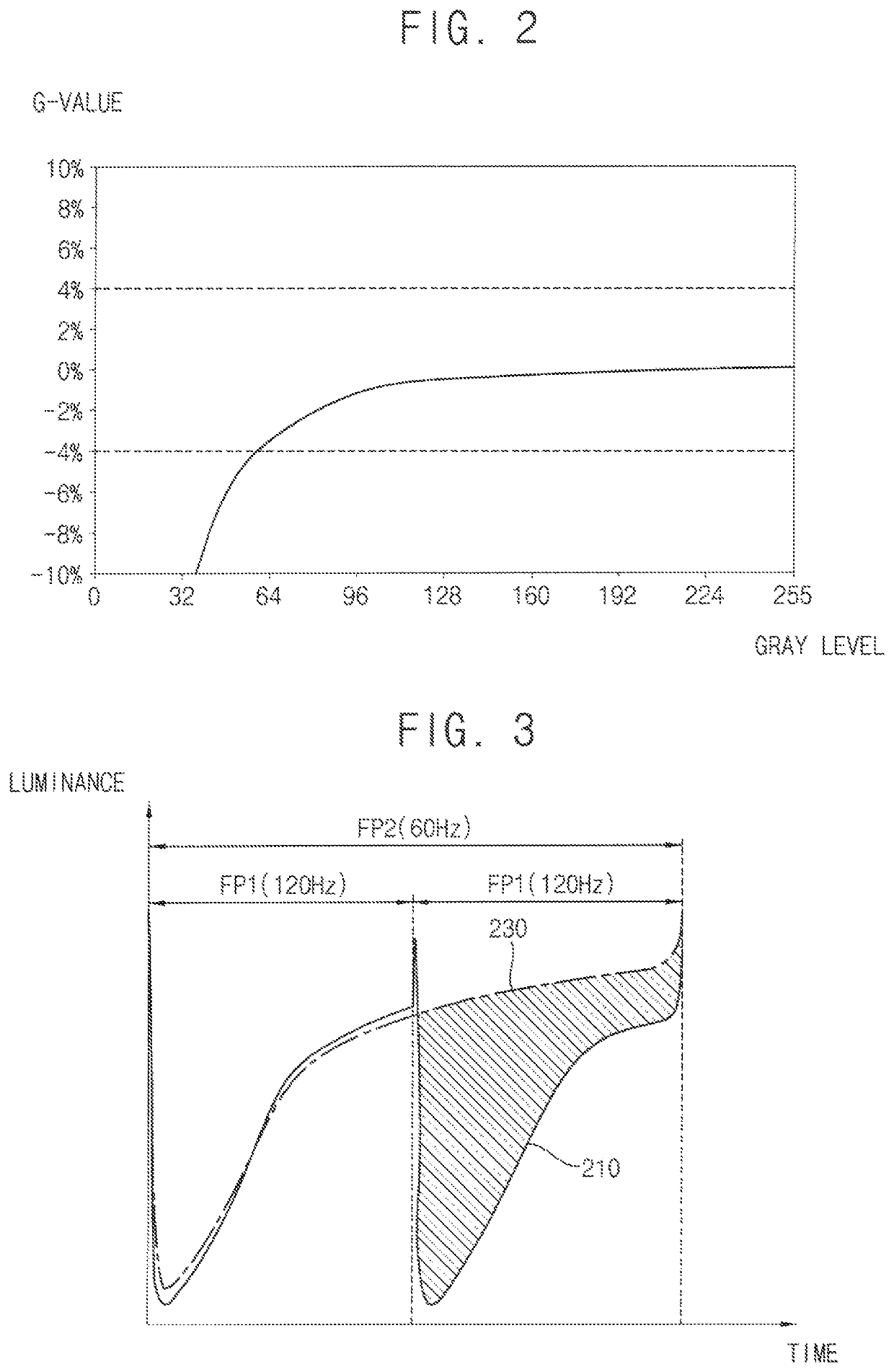
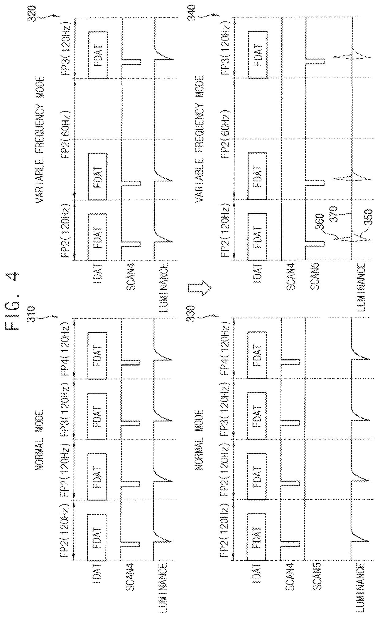
However, in the OLED display device operated at the variable frequency mode, a luminance of the display panel driven at a first driving frequency and a luminance of the display panel driven at a second driving frequency different from the first driving frequency may be different from each other, and thus a flicker may occur when a driving frequency of the display panel is changed.

Method used


Image

  • Pixel of an organic light emitting diode display device, and organic light emitting diode display device
  • Pixel of an organic light emitting diode display device, and organic light emitting diode display device
  • Pixel of an organic light emitting diode display device, and organic light emitting diode display device

Examples


Embodiment Construction

[0061]Hereinafter, embodiments of the present inventive concept will be explained in detail with reference to the accompanying drawings.

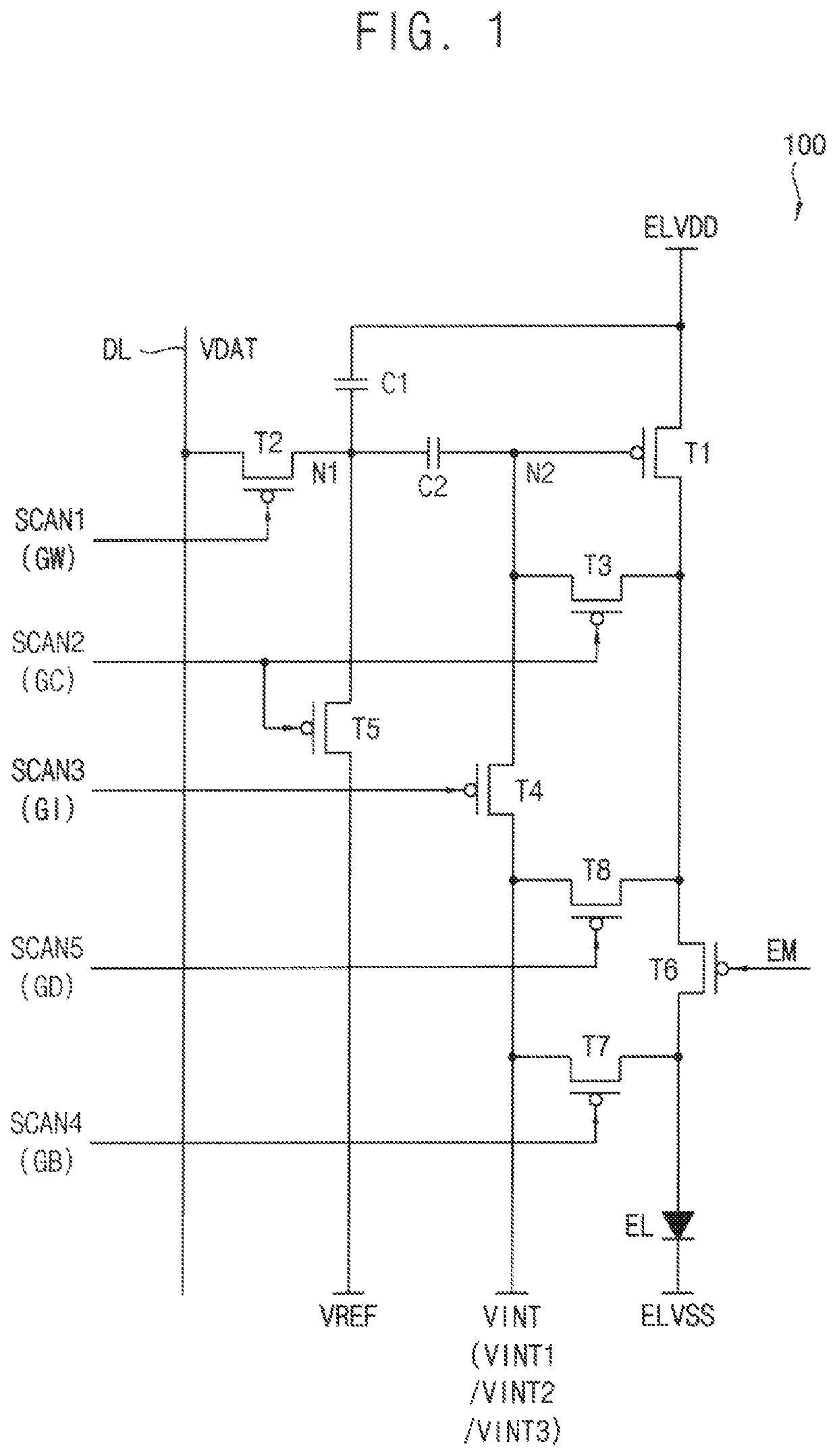
[0062]FIG. 1 is a circuit diagram illustrating a pixel of an organic light emitting diode (OLED) display device according to embodiments, FIG. 2 is a diagram illustrating an example of a G-value of a conventional display panel in which each pixel initializes an OLED in each frame period, FIG. 3 is a diagram illustrating an example of a luminance of a conventional display panel driven at a frame frequency of about 120 Hz, and an example of a luminance of the conventional display panel driven at a frame frequency of about 60 Hz, and FIG. 4 is a diagram illustrating an example of a luminance of a conventional display panel in a normal mode, an example of a luminance of the conventional display panel in a variable frequency mode, an example of a luminance of a display panel in the normal mode according to embodiments, and an example of a luminance of th...


PUM

PropertyMeasurementUnit
frequencyaaaaaaaaaa
frequencyaaaaaaaaaa
frequencyaaaaaaaaaa

Abstract

A pixel of an OLED display device includes a first capacitor, a second capacitor, a first transistor configured to generate a driving current, a second transistor configured to transfer a data voltage to a first node, a third transistor configured to diode-connect the first transistor, a fourth transistor configured to transfer an initialization voltage to the second node, a fifth transistor configured to transfer a reference voltage to the first node, a sixth transistor configured to couple a drain of the first transistor and an anode of an organic light emitting diode, a seventh transistor configured to transfer the initialization voltage to the anode of the organic light emitting diode, an eighth transistor configured to transfer the initialization voltage to the drain of the first transistor, and the organic light emitting diode.

Description

CROSS-REFERENCE TO RELATED APPLICATION(S)[0001]This application claims priority under 35 USC § 119 to Korean Patent Application No. 10-2020-0116816, filed on Sep. 11, 2020, in the Korean Intellectual Property Office (KIPO), the disclosure of which is incorporated by reference herein in its entirety.BACKGROUND1. Field[0002]Embodiments of the present inventive concept relate to a display device, and more particularly to a pixel of an organic light emitting diode (OLED) display device, and the OLED display device.2. Description of the Related Art[0003]In general, an OLED display device may display an image at a fixed frame frequency (or a constant refresh rate) of about 60 Hz, about 120 Hz, about 240 Hz, or the like. However, a frame frequency of a host processor (e.g., a graphic processing unit (GPU) or a graphic card) providing frame data to the OLED display device may be different from the frame frequency of the OLED display device. In particular, when the host processor provides th...

Claims


Application Information

Patent Timeline
Patent Type & Authority Patents(United States)
IPC IPC(8): G09G3/3291G09G3/3266G09G3/3233G09G3/3208
CPCG09G3/3291G09G3/3266G09G2300/0819G09G2310/061G09G2310/08G09G3/3208G09G2320/0233G09G3/3233G09G2300/0852G09G2300/0861G09G2320/0238G09G2340/0435G09G2320/0247G09G2310/0251G09G3/325G09G3/3275
Inventor KIM, JIHYEJIN, JAKYOUNGKIM, YU-CHOLYANG, JIN-WOOK
Owner SAMSUNG DISPLAY CO LTD
Learn More