Eureka AIR delivers breakthrough ideas for toughest innovation challenges, trusted by R&D personnel around the world.

Semiconductor memory device

Inactive Publication Date: 2002-01-03
CONTEC CO LTD
View PDF0 Cites 7 Cited by
  • Summary
  • Abstract
  • Description
  • Claims
  • Application Information

AI Technical Summary

Benefits of technology

[0011] Still another object of the present invention is to provide a semiconductor memory device as a non-volatile memory that can be easily mounted in a variety of electronic equipment.
[0012] It is still another object of the present invention to provide a semiconductor memory device which can be quickly and easily installed as a replacement for a hard disk device.
[0013] Yet another object of the present invention is to avoid the need of additional mounting equipment to adapt the semiconductor memory device to the mounting configuration of various hard disk device types.
[0014] Briefly stated, the present invention provides a single semiconductor memory device replaces a variety of hard disk device types having different mounting configurations. The semiconductor memory device must have available the same mounting configuration as that of the hard disk device. Including multiple mounting configuration means, such as screw holes, in the case of the semiconductor memory device avoids the need for multiple replacement semiconductor memory device types. The multiple mounting configurations allow the semiconductor memory device to be mounted in a variety of orientations and mounting configurations. Thus, a single semiconductor memory device type can replace multiple varieties of hard disk device types without the need for extra mounting equipment.

Problems solved by technology

The disk is subject to vibration as a result of the high rate of rotation.
These vibrations can damage the disk or cause impact between the disk surface and the read / write head(s) which access disk data.

Method used


Image

  • Semiconductor memory device
  • Semiconductor memory device
  • Semiconductor memory device

Examples


Embodiment Construction

[0027] Referring first to FIG. 7(a), one type of an internal hard disk device 2 is shown that acts as a non-volatile memory storage device in a piece of electronic equipment, in this case a notebook type personal computer 1. Hard disk device 2 is oriented with its long dimension perpendicular to the long dimension of personal computer 1.

[0028] Referring to FIG. 5, hard disk device 2 is mounted and attached to a base 4 by a plurality of screws 3. Base 4 is placed in the interior of notebook type personal computer 1.

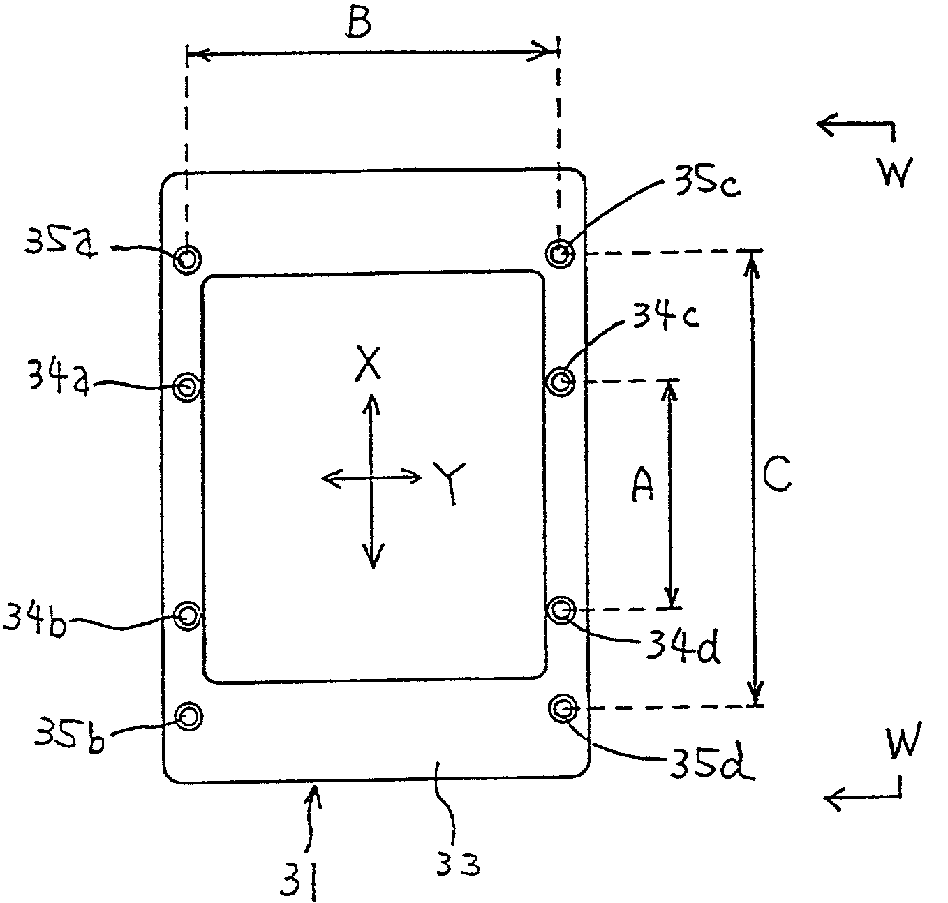
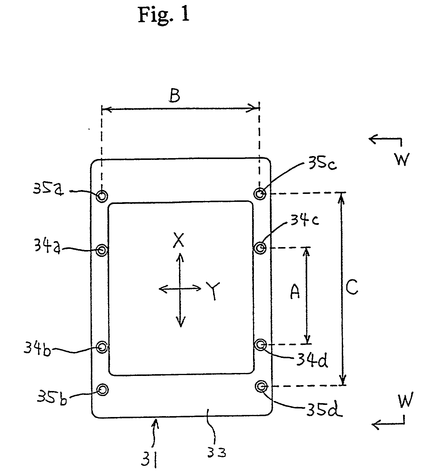
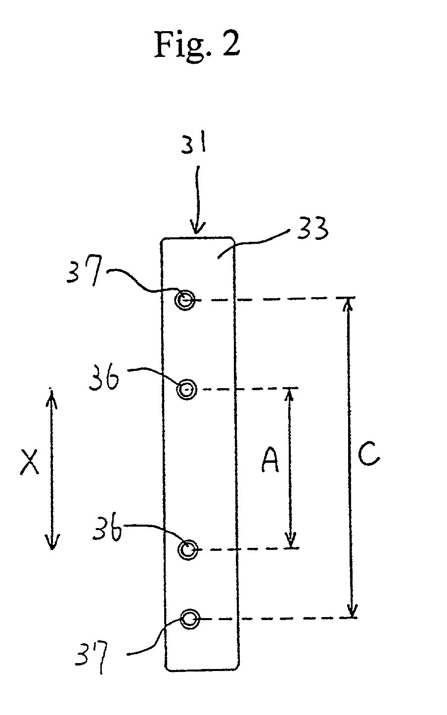
[0029] A plurality of mounting screw holes 6a-6d are formed in a case 5 of hard disk device 2. Screw passage holes 7a-7d are formed in base 4 and align with each mounting screw hole 6a-6d. Each of mounting screw holes 6a-6d and screw passage holes 7a-7d are formed so that there is a spacing A in the X-direction and a spacing B in the Y-direction.

[0030] Hard disk device 2 is placed in a mounting position on base 4. Each mounting screw hole 6a-6d is aligned with a correspond...


PUM


Abstract

A single semiconductor memory device replaces a variety of hard disk device types having different mounting configurations. The semiconductor memory device must have available the same mounting configuration as that of the hard disk device. Including multiple mounting configuration means, such as screw holes, in the case of the semiconductor memory device avoids the need for multiple replacement semiconductor memory device types. The multiple mounting configurations allow the semiconductor memory device to be mounted in a variety of orientations and mounting configurations. Thus, a single semiconductor memory device type can replace multiple varieties of hard disk device types without the need for extra mounting equipment.

Description

[0001] The present invention is a continuation in part of Provisional Application Serial No. 60 / 068,482, filed Dec. 22, 1997.BACKGROUND OF THE INVENTION[0002] The present invention relates to a semiconductor memory device which can be exchanged with a variety of models of hard disk devices used with electronic equipment.[0003] Personal computers and other devices requiring large capacity non-volatile storage have traditionally incorporated internal hard disks in their architecture. As shown in FIG. 8, a conventional hard disk device 41 is generally mounted to a base 43 inside a personal computer (not shown). A plurality of mounting screw holes 45a-45d are formed on a case 44 of hard disk device 41. Base 43 has a plurality of screw passage holes 46a-46d which align with each mounting screw hole 45a-45d. A plurality of screws 42 pass through the aligned screw holes to mount hard disk device 41 to base 43 inside the computer.[0004] The prior art includes a disk (not shown) inside inter...

Claims


Application Information

Patent Timeline
IPC IPC(8): G11C5/00
CPCG06F1/187
Inventor HAYANO, SHIRONISHIYAMA, KAZUYOSHI
Owner CONTEC CO LTD
Why Eureka
Eureka Blog
Learn More