

Device mounting method and device transport apparatus
- Summary
- Abstract
- Description
- Claims
- Application Information
AI Technical Summary
Benefits of technology
Problems solved by technology
Method used
Image

Examples
first embodiment
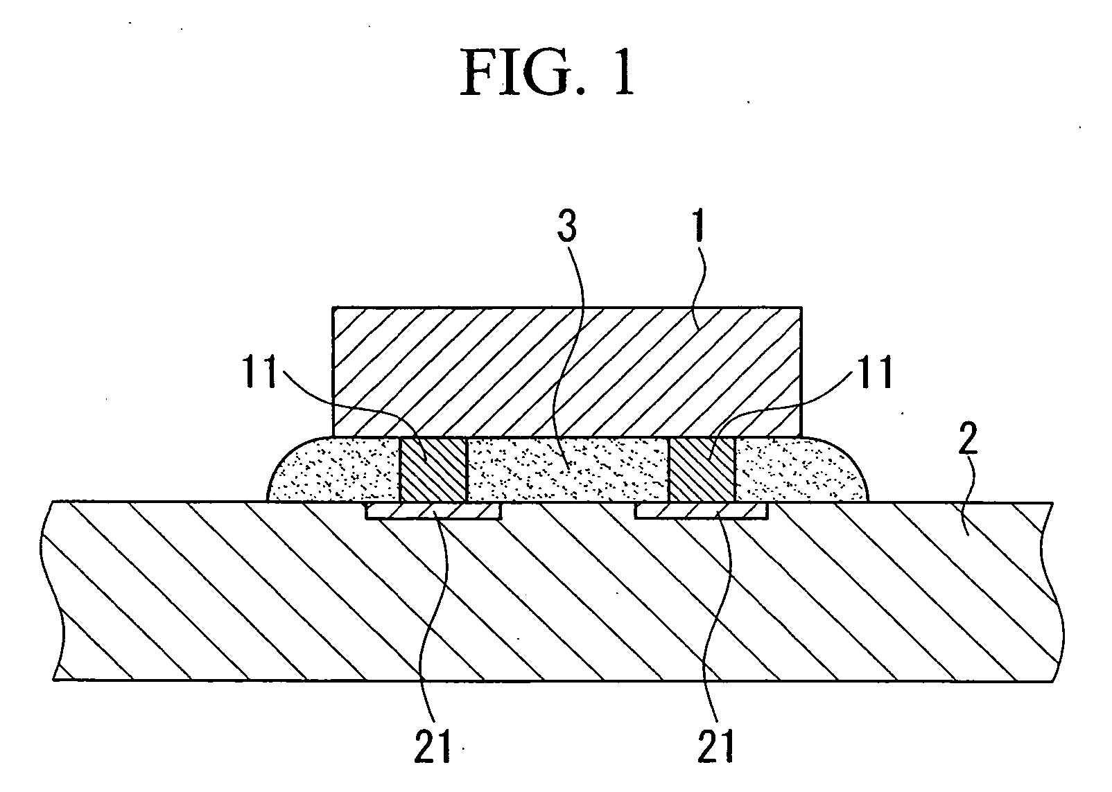
[0028] Next, an explanation of a mounting method for mounting the micro-semiconductor chip 1 on circuit board 2 will be made hereinafter.
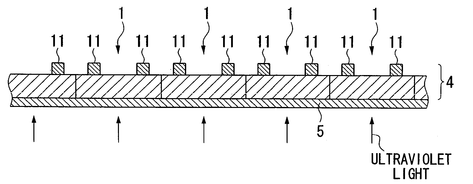
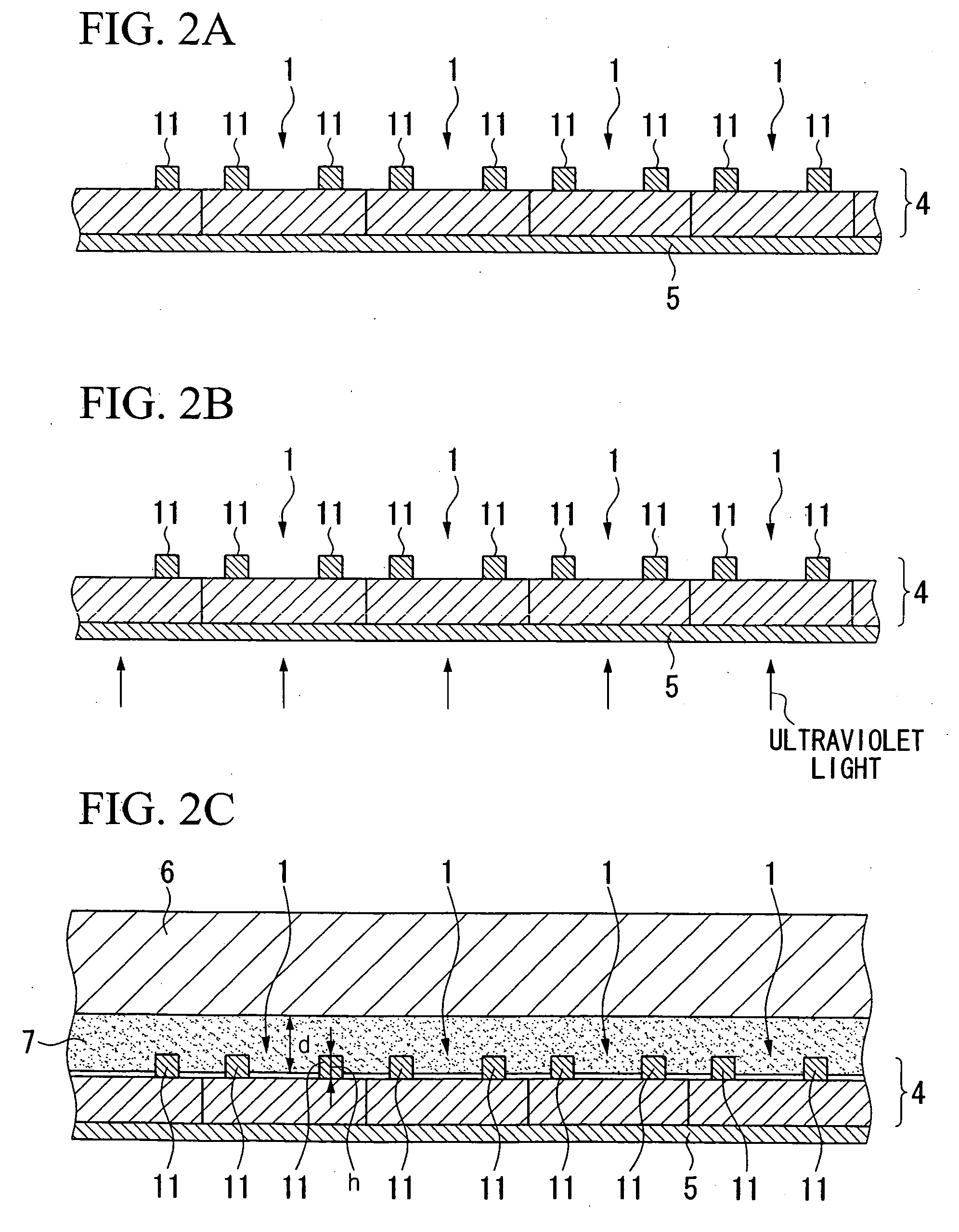
[0029] First, as shown in FIG. 2A, a semiconductor wafer 4 composed of silicon and so forth is arranged on a dicing sheet 5 coated with an ultraviolet-cured resin. The semiconductor wafer 4 is divided into a plurality of sections by a diamond blade or laser beam to form micro-semiconductor chips 1. Subsequently, as shown in FIG. 2B, the ultraviolet light is irradiated from the lower side, that is, from the side where the dicing sheet 5 is provided. The adhesive strength of the ultraviolet-cured resin is thus reduced by irradiating with the ultraviolet light. A plurality of bumps 11 corresponding to each micro-semiconductor chip 1 are formed in advance on the side of semiconductor wafer 4 not having a dicing sheet. More specifically, a plurality of bumps 11 are provided on the upper side of the semiconductor wafer 4 in the drawing, that is, the bum...
second embodiment
[0041] In the device mounting method of the second embodiment, as shown in FIG. 4A, a transfer substrate 6 coated with solder 9 is pressed against the semiconductor wafer 4 attached with the dicing sheet 5. When pressing the transfer substrate 6 against the semiconductor wafer 4, the solder 9 is softened by heating the transfer substrate 6 to a degree that it does not run off when the transfer substrate 6 is inverted. Thickness D of the solder 9 is coated on the transfer substrate 6 by preferably less than the height h of the bumps 11 possessed by each micro-semiconductor chip 1. By making the thickness D of the solder 9 less than the height h of the bumps 11 in this manner, short-circuiting between the circuit of the micro-semiconductor chips 1 and adjacent bumps 11 can be inhibited. By pressing the transfer substrate 6 coated with solder 9 against the semiconductor wafer 4 in this manner, an intermetallic compound is formed on the surface of the bumps 11.
[0042] Subsequently, the t...
third embodiment
[0051] According to the device transport apparatus 100 of the third embodiment, the transport apparatus 100 is provided with the transfer substrate transport apparatus 110 that transports the transfer substrate 6. The micro-semiconductor chips 1 can be, therefore, easily transferred to the transfer substrate 6, and additionally transported to the bonding apparatus.
[0052] In addition, according to the transport apparatus 100 of the third embodiment, the transport apparatus 100 is provided with the transfer substrate inversion apparatus 120. Therefore, the transfer substrate 6 to which the micro-semiconductor chips 1 have been transferred can be transported to the bonding device after being inverted.
[0053] While the preferred embodiments of the device mounting method and the device transport apparatus according to the present invention have been described and illustrated above, it should be understood that these are exemplary of the present invention and are not to be considered as l...
PUM
 Abstract
Description
Claims
Application Information