Post CMP clean brush with torque monitor

a technology of torque monitor and clean brush, which is applied in the direction of carpet cleaner, instruments, photosensitive materials, etc., can solve the problems of shortening the ic device, affecting the yield and chip performance, and reducing the efficiency of protruding protrusions on the surfa

Inactive Publication Date: 2002-01-17
AGILENT TECH INC
View PDF0 Cites 36 Cited by
  • Summary
  • Abstract
  • Description
  • Claims
  • Application Information

AI Technical Summary

Problems solved by technology

As more layers are built up on the silicon wafer, problems caused by surface non-planarity become increasingly severe and can impact yield and chip performance.
Protrusions on the surface erode more efficiently than recessed areas leading to a flattening or planarization of the wafer surface.
Any residue remaining on the wafer can cause shorts to the IC devices.
The problem associated with the DNS brush cleaner is the inability of the machine to recognize whether the brush has fallen off and is not making contact with the wafer.
A tool user cannot actually see that the brush has fallen off the brush holder since the cleaning process is within an enclosed chamber.
Also problems arise when the brush's contact pressure is improperly set during maintenance set up or during the brush cleaning cycle.
The silent failure of the brush to properly clean the wafer is difficult to detect until the next inspection point.
At that time, several wafer lots have gone through the brush cleaner and would require reworking the lots, a costly solution.
This patent does not disclose or suggest monitoring the torque as a means to detect the presence of the abrading tool but rather as a means to adjust the contact pressure of the tool.
However, this patent discloses adjusting the contact pressure of the tool on the surface being maintained and does not disclose or suggest using the torque value as an input to detecting the presence of the tool itself.

Method used


Image

  • Post CMP clean brush with torque monitor
  • Post CMP clean brush with torque monitor
  • Post CMP clean brush with torque monitor

Examples


Embodiment Construction

)

[0037] In describing the preferred embodiment of the present invention, reference will be made herein to FIGS. 1-2B of the drawings in which like numerals refer to like features of the invention. Features of the invention are not necessarily shown to scale in the drawings.

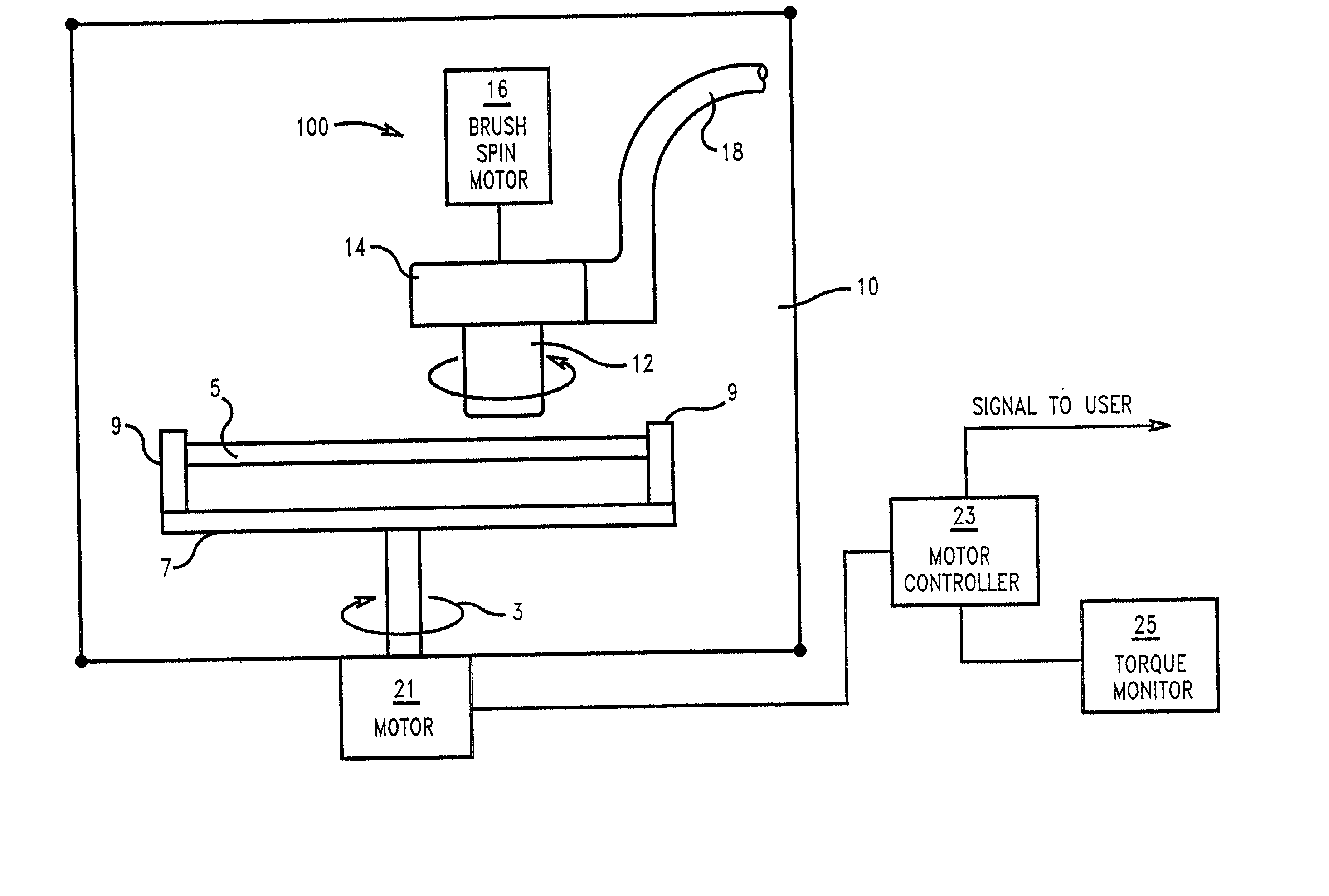
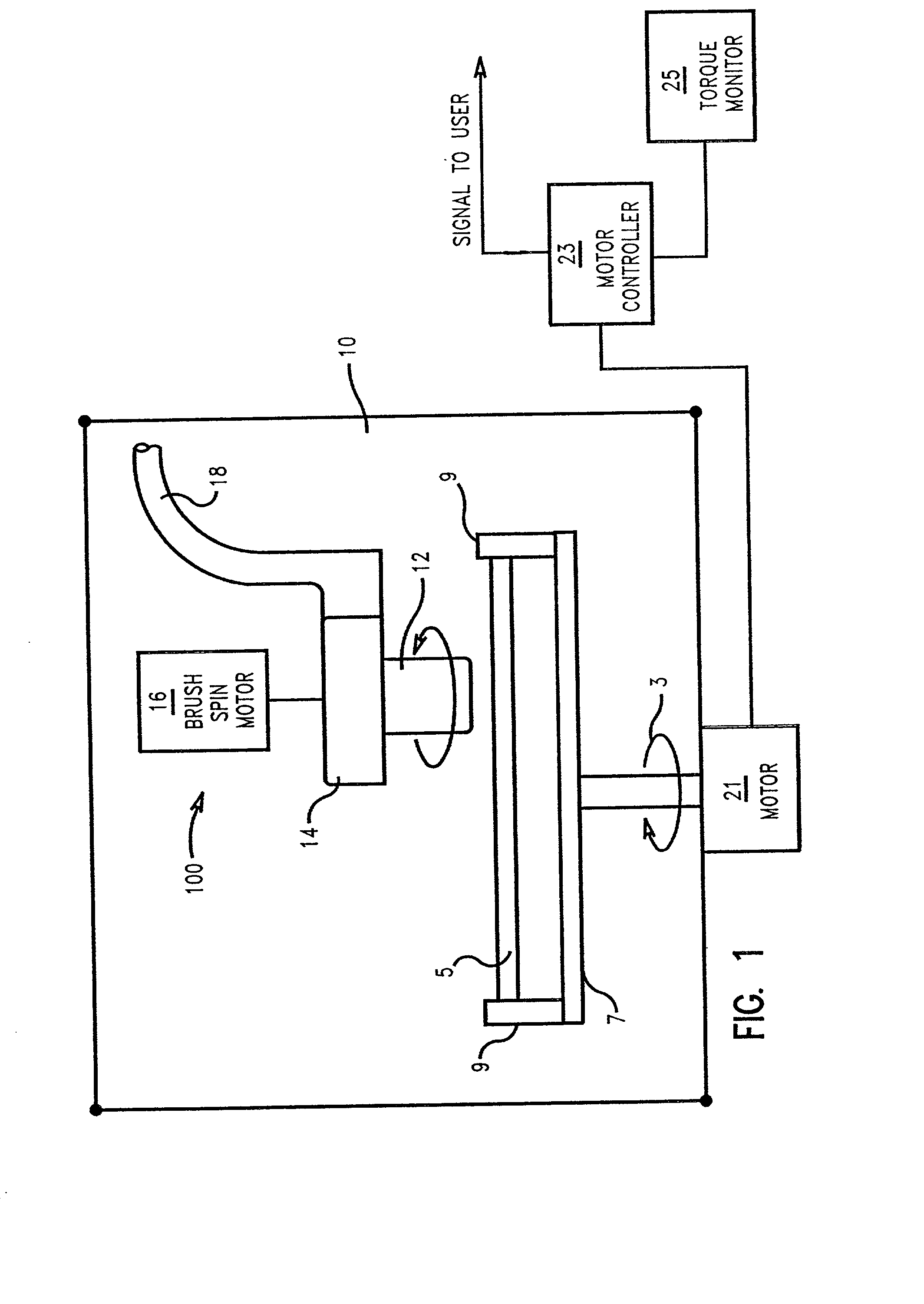
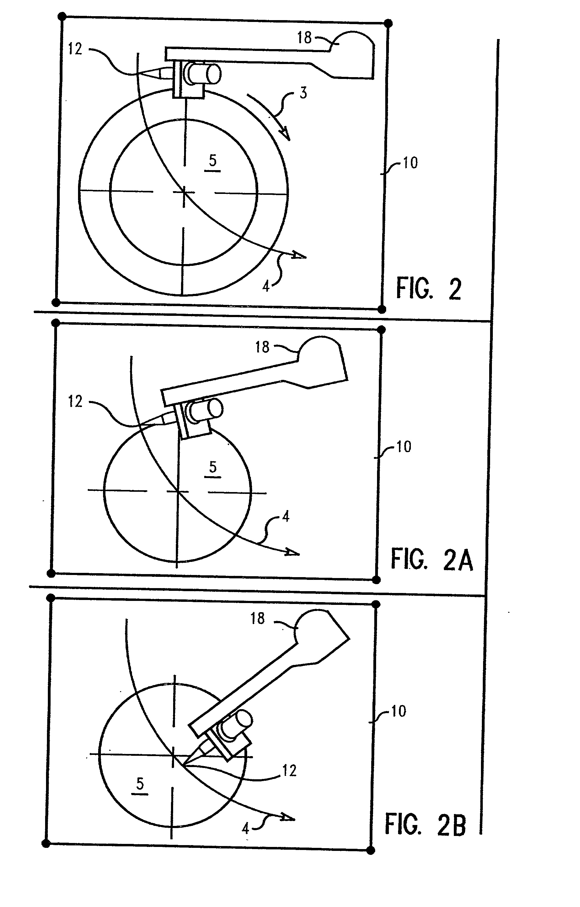
[0038] In connection with the instant invention, it has been discovered that during the brush cleaning cycle, the wafer experiences a torque which is directly proportional to the brush friction of the brush against the wafer. At constant spin speed, the torque on the wafer increases as the brush moves radially outward. Cleaning is achieved by the turbulent interaction between the brush and the wafer surface. If the brush is not making contact with the wafer, the only torque experienced by the wafer is due to air and water friction, and the friction due to the mechanical drive motor. Conversely, when the brush is applied with too much force, the torque excursion during the brush clean cycle is extreme.

[0039] FIG. 1...


PUM


Abstract

An apparatus for and method of detecting the presence of a brush used in a semiconductor wafer cleaner for post-CMP processing is described. Semiconductor wafers are loaded into the wet environment of the wafer cleaner, affixed to a rotatable fixture and rotated at high speed. The rotatable fixture is effectuated by a servo motor linked to a servo controller and a torque monitor. A first torque on the rotating wafer is calculated prior to the start of the brush cleaning cycle. During the brush cleaning cycle, as the brush within the brush cleaner contacts the rotating wafer, the torque on the wafer increases and a second torque is calculated. If, during the brush cleaning cycle, the second torque calculation is substantially equal to the first torque calculation, the brush cleaner is not contacting the wafer and cleaning has not progressed. A tool user can be notified to reaffix the brush within the cleaner. When the second torque calculation is greater than expected, the tool user can be notified that the brush downforce has been improperly set. Inadequate removal of CMP residue is detected before entire wafer lots have passed through an ineffective brush cleaning cycle prior to an inspection point.

Description

[0001] 1. Field of the Invention[0002] This invention relates, in general, to the field of semiconductor manufacture. In particular, it relates to monitoring the conditions of post chemical mechanical polishing processing.[0003] 2. Description of Related Art[0004] Fabrication of semiconductor integrated circuits (IC) is a complicated multi-step process for creating microscopic structures with various electrical properties to form a connected set of devices. As the level of integration of ICs increases, the devices become smaller and more densely packed, requiring more levels of photolithography and more processing steps. As more layers are built up on the silicon wafer, problems caused by surface non-planarity become increasingly severe and can impact yield and chip performance. During the fabrication process, it may become necessary to remove excess material in a process referred to as planarization.[0005] A common technique used to planarize the surface of a silicon wafer is chemi...

Claims


Application Information

Patent Timeline
Patent Type & Authority Applications(United States)
IPC IPC(8): H01L21/00
CPCH01L21/67046H01L21/67253H01L21/67259Y10S134/902
Inventor BEARDSLEY, GARY J.BULLARD, TIMOTHY S.HUYNH, CUC KIMVAN KESSEL, THEODORE G.WALKER, DAVID L.
Owner AGILENT TECH INC
Why Eureka
Try Eureka