Scan based multiple ring oscillator structure for on-chip speed measurement

a technology of speed measurement and multiple ring oscillator, applied in the direction of measuring devices, instruments, generating/distributing signals, etc., can solve the problems of not exporting their information outside of the chip, affecting the speed of parts at wafer test, and delay in broadside speed testing

Inactive Publication Date: 2002-09-12
HEWLETT PACKARD DEV CO LP
View PDF6 Cites 102 Cited by
  • Summary
  • Abstract
  • Description
  • Claims
  • Application Information

AI Technical Summary

Benefits of technology

0005] The present invention bundles four ring oscillators, a 20-bit ripple counter and the necessary control logic needed to implement a Joint Test Action Group (JTAG) scan based interface. The present system can be located on every die, so that each location can

Problems solved by technology

Due to the limitations of wafer testing, broadside speed testing is usually delayed until the dies are packaged.
Thus, it is often difficult to know the speed of a part at wafer test.
There are other ring oscillator structures placed on

Method used


Image

  • Scan based multiple ring oscillator structure for on-chip speed measurement
  • Scan based multiple ring oscillator structure for on-chip speed measurement
  • Scan based multiple ring oscillator structure for on-chip speed measurement

Examples


Embodiment Construction

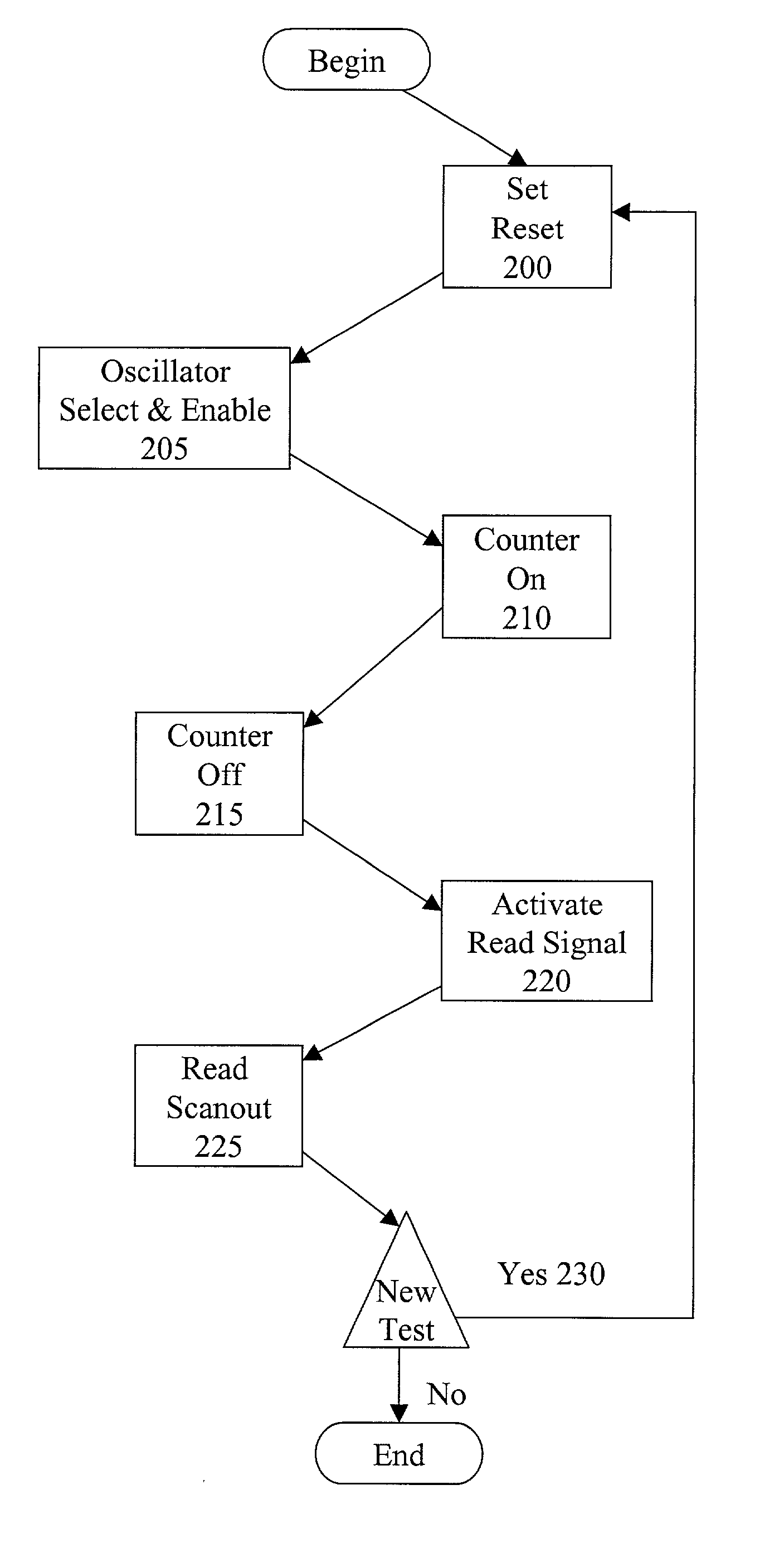
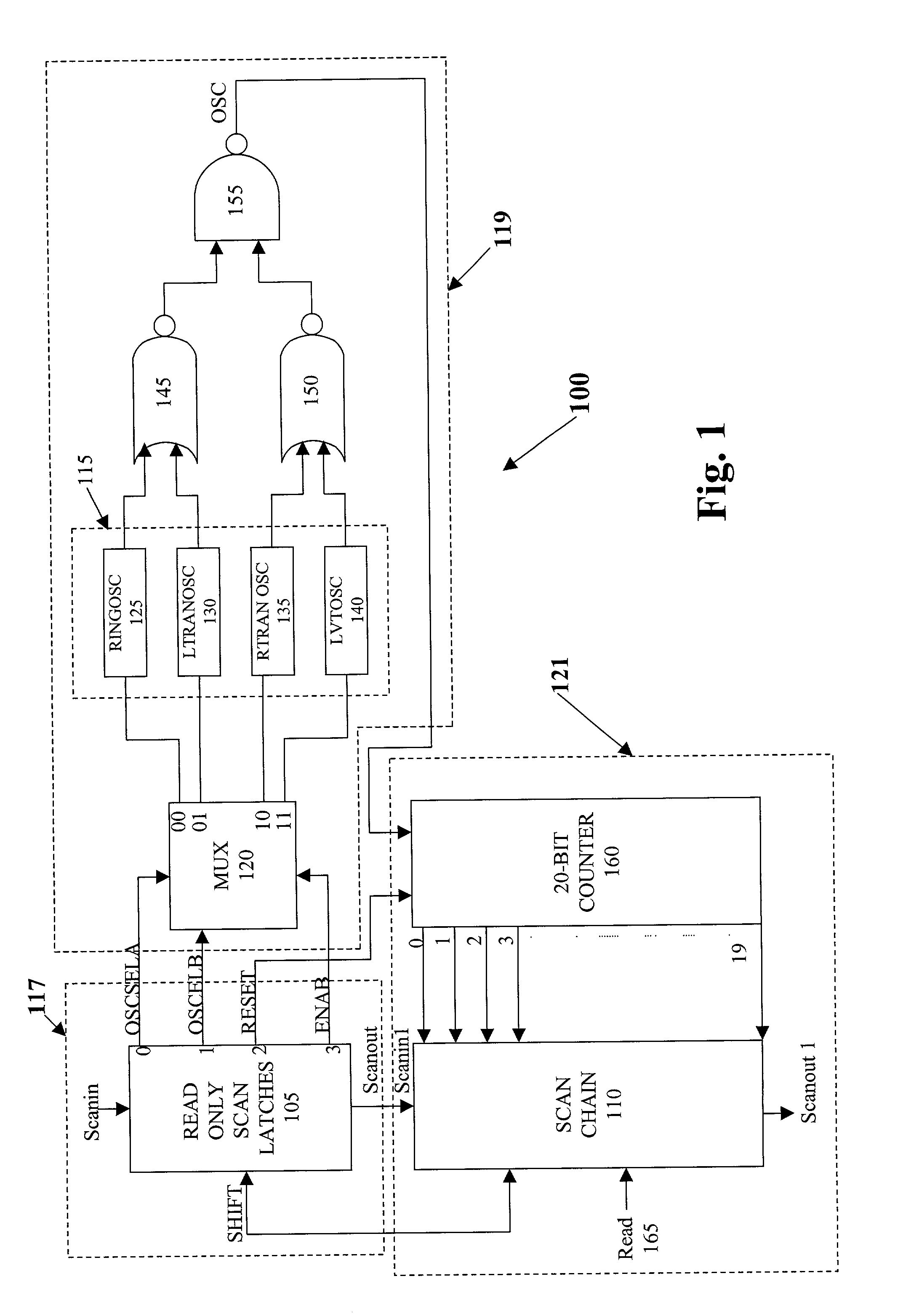
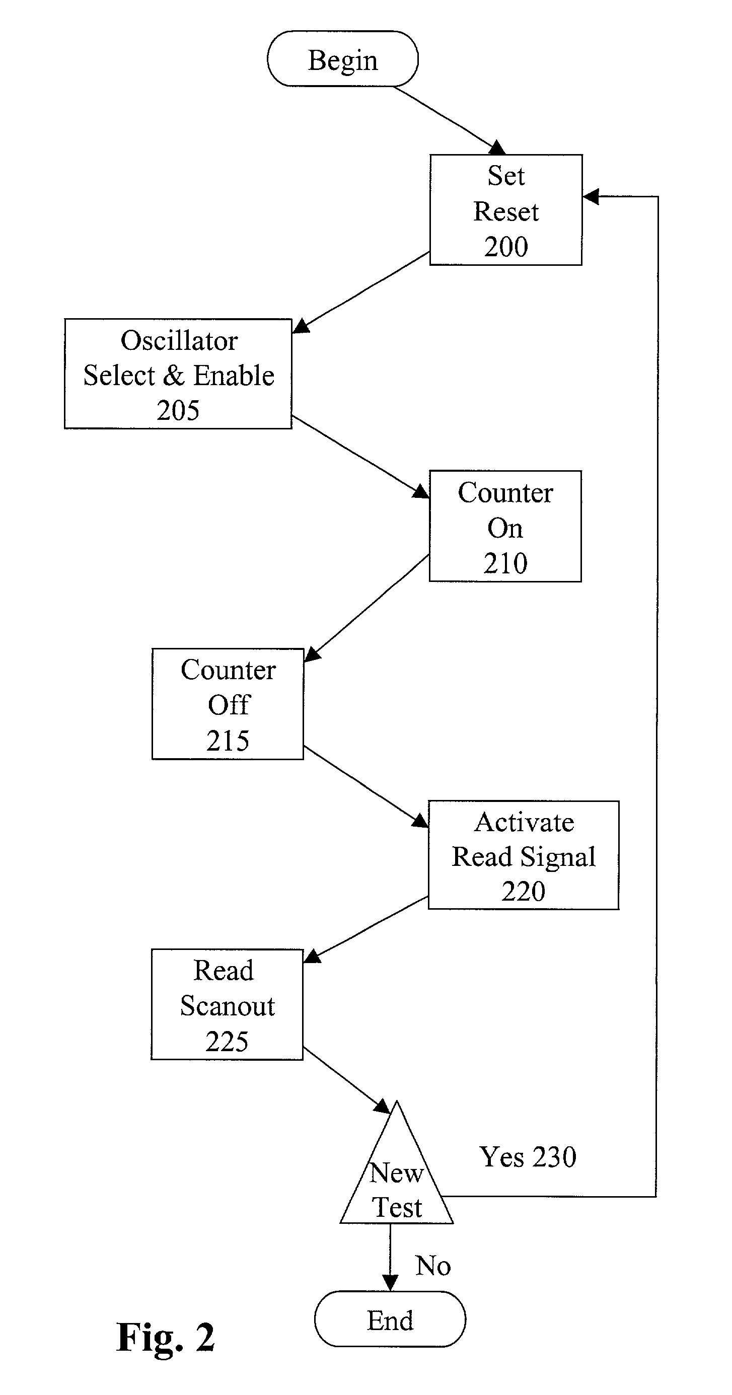
[0009] FIG. 1 illustrates a system 100 that tracks process variations. Circuit 117 includes read only scan latches 105 that contain four control bits. The function of the circuit is for clock and count control. The circuit 117 controls which one of the clocks is going to run. The four control bits of the scan latches are BIT 0--OSCSELA, BIT 1--OSCSELB, BIT 2--RESET and BIT3--ENAB. In addition to the four control bits, the scan latches 105 also includes two inputs signals: SHIFT clock and SCAN IN, and an output signal SCAN OUT.

[0010] Circuit 121 includes scan chain 110 that contains 20 scan bits used to scan out a final count of a 20-bit counter 160. The function of circuit 121 is to count the clock and capture the count onto the scan chain 110. The system 100 uses the SHIFT signal to transfer all the data into scan latches 105 and out of the scan chain 110. By controlling the SCANIN signal in conjunction with the SHIFT signal, control bits can be loaded into the scan latches 105 or ...


PUM


Abstract

The present invention bundles four ring oscillators, a 20-bit ripple counter and the necessary control logic needed to implement a JTAG scan based interface. The present system can be located on every die, so that each location can be individually tested. It communicates with the outside world through a standard JTAG interface. It is accessible at wafer, package, and system test which allows for several methods of correlating the oscillator speed to the speed of a part in the actual system.

Description

TECHNICAL FIELD[0001] The technical field is tracking process variations.BACKGROUND ART[0002] Ring oscillators are often used in analog parameter testing (APT) structures generated by wafer manufacturers. The manufacturer makes a wafer and different dies sit on the wafer. One important function is to try and optimize the number of dies placed on one wafer. To save space, manufacturers place the APT structures in the area between two dies.[0003] Speed banning is usually done based upon some type of broadside test performed by a package tester. These tests are run by the fabrication which saves the information in a database. Due to the limitations of wafer testing, broadside speed testing is usually delayed until the dies are packaged. Thus, it is often difficult to know the speed of a part at wafer test. There are other ring oscillator structures placed on a chip to attempt to compensate for process variation, however, none of them export their information outside of the chip.[0004] ...

Claims


Application Information

Patent Timeline
IPC IPC(8): G01R31/3185
CPCG01R31/31858
Inventor HUTTON, JOHN F.HUDSON, WILLIAM A.HALPERIN, DANIEL L.KRUEGER, DANIEL W.LAVIER, JACK T.MUSGROVE, MARK D.
Owner HEWLETT PACKARD DEV CO LP
Why Eureka
Try Eureka