Optical substrate having alignment fiducials

Inactive Publication Date: 2002-10-17
TYCO ELECTRONICS LOGISTICS AG (CH)
View PDF6 Cites 5 Cited by
  • Summary
  • Abstract
  • Description
  • Claims
  • Application Information

AI Technical Summary

Benefits of technology

0007] The present invention provides for an optical substrate having highly precise alignment features for receiving and aligning optical components thereon. The accuracy and precision realized by the substrate of the present invention is due to a single masking step which defines all the critical alignment features on the substrate. Traditionally, this was not possible because the various alignment features were formed with totally different processes requiring different conditions and separate masking

Problems solved by technology

Traditionally, this was not possible because the various alignment features were formed with totally different processes requiring different conditions and separate masking steps.
Additionally, th

Method used


Image

  • Optical substrate having alignment fiducials
  • Optical substrate having alignment fiducials
  • Optical substrate having alignment fiducials

Examples


Embodiment Construction

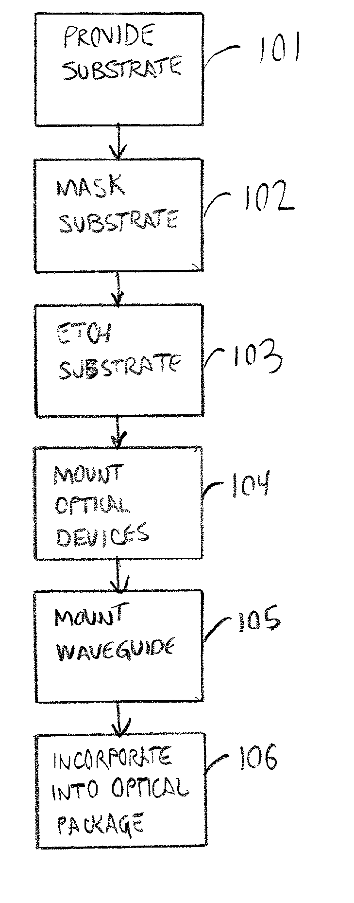
[0018] Referring to FIG. 1, a flow chart of the process of the present invention is shown indicating the steps for preparing a substrate with alignment features. As used herein, the term "alignment features" refers to contours in the substrate formed by etching which are adapted to receive a waveguide and at least one optical device and align them on the substrate such that they are optically coupled. It should be understood that optical coupling may be achieved directly by coaxially aligning the optical axes of the optical device and waveguide or indirectly by using a light bending device such as a prism to couple the optical axes of the components. Typical alignment features include, for example, a groove for receiving a waveguide, such as a fiber, and fiducials for providing a reference surface for placing an optical device, such as a laser die, on the substrate in precise alignment with the waveguide.

[0019] In step 101, a suitable substrate is provided for contouring alignment f...


PUM


Abstract

A process comprising: (a) applying a stop etch mask to a substrate, the mask defining the location on the substrate of a groove for receiving a waveguide and one or more fiducials for positioning the optical device on the substrate relative to the waveguide; and (b) etching the substrate to define the fiducials and the groove, the groove being dimensioned to receive at least a portion of a waveguide and the fiducials enabling the optical device to be positioned on the substrate such that it is optically aligned with the waveguide.

Description

[0001] The application is based upon Provisional Application No. 60 / 238,815, filed Oct. 6, 2000, and hereby incorporated by reference.[0002] This invention relates generally to optical substrates, and, more particularly, to optical substrates having alignment features for aligning optical components thereon.BACKGROUND OF INVENTION[0003] It is well known to align optical components on a silicon substrate using register surfaces as mechanical stops. In this approach, an optical device, such as a laser, is precisely aligned to a silicon wafer surface by butting a precision notch surface of the laser against a mechanical stop or pedestal protruding from the silicon wafer board surface. The height of the laser or optical device is determined by the height of a separate etched standoff positioned under the laser on the wafer surface. An optical fiber, intended to be optically aligned to that laser, is registered to the silicon wafer board by bonding it to a precision-etched V-groove. Beca...

Claims


Application Information

Patent Timeline
IPC IPC(8): G02B6/42H01L21/302H01L21/461
CPCG02B6/4228
Inventor BOUDREAU, ROBERT ADDISONDRABENSTADT, CHRISTIANSCHRAMM, JEFFERY EMERSON
Owner TYCO ELECTRONICS LOGISTICS AG (CH)
Why Eureka
Try Eureka