

Electroless plating liquid and semiconductor device
Inactive Publication Date: 2002-12-12
EBARA CORP
View PDF0 Cites 61 Cited by
- Summary
- Abstract
- Description
- Claims
- Application Information
AI Technical Summary
Problems solved by technology
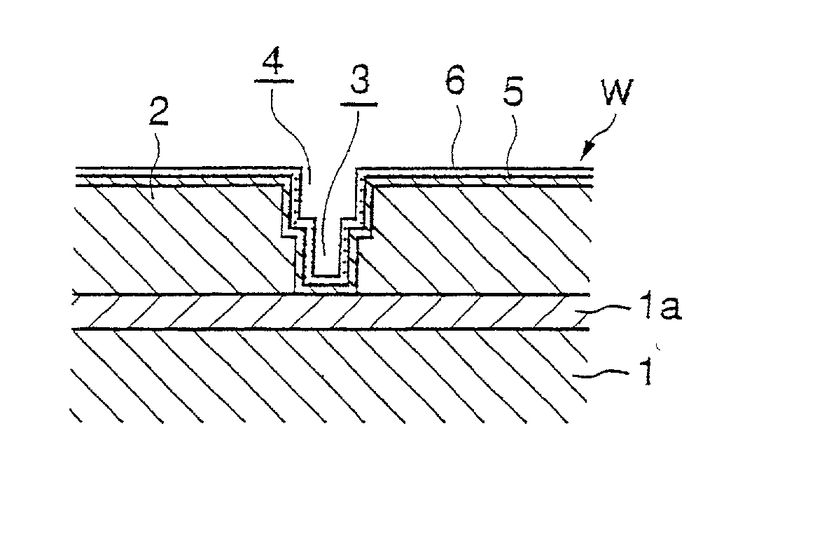
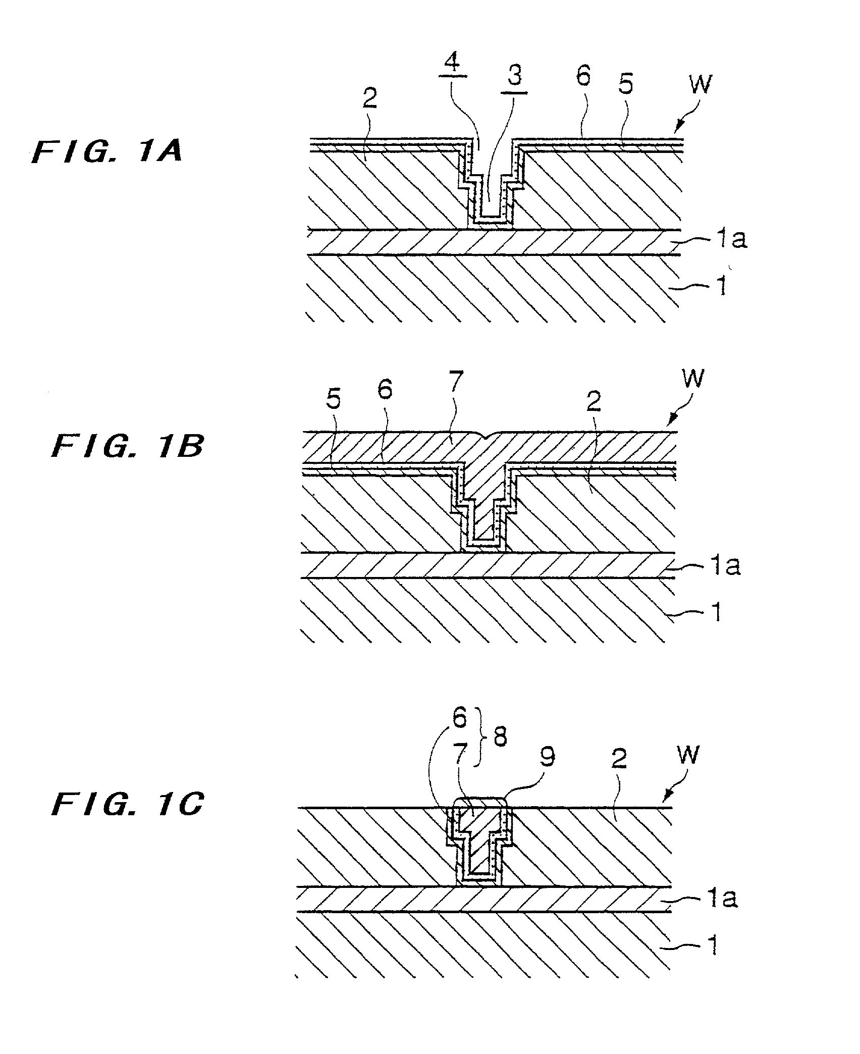
When an additional embedded interconnect structure is formed on such an interconnects-exposing surface of a semiconductor substrate, the following problems may be encountered.
Further, upon etching of the SiO.sub.2 layer for formation of via holes, the pre-formed interconnects exposed on the bottoms of the via holes can be contaminated with an etchant, a peeled resist, etc.
However, the provision of a protective film of SiN or the like on the whole surface of a semiconductor substrate, in a semiconductor device having an embedded interconnect structure, increases the dielectric constant of the interlevel dielectric, thus inducing interconnect delaying even when a low-resistance material such as copper or silver is employed for interconnects, whereby the performance of the semiconductor device may be impaired.
The provision of such a protective alloy film by electroless plating, however, has the following problems associated with sodium hypophosphite which is generally used as a reducing agent in electroless plating:
{circle
Method used
View moreImage
Smart ImageViewing Examples

Examples
 PUM
| Property | Measurement | Unit |
|---|---|---|
| Thickness | aaaaa | aaaaa |
| Acidity | aaaaa | aaaaa |
| Refractory | aaaaa | aaaaa |
Abstract
The present invention relates to an electroless-plating liquid useful for forming a protective film for selectively protecting the surface of the exposed interconnects of a semiconductor device which has such an embedded interconnect structure that an electric conductor, such as copper or silver, is embedded in fine recesses for interconnects formed in the surface of a semiconductor substrate, and to a semiconductor device in which the surface of the exposed interconnects is selectively protected with a protective film. The electroless-plating liquid contains cobalt ions, a complexing agent and a reducing agent containing no alkali metal.
Description
[0001] 1. Field of the Invention[0002] This invention relates to an electroless-plating liquid and a semiconductor device. More particularly, this invention relates to an electroless-plating liquid useful for forming a protective film for selectively protecting the surface of the exposed interconnects of a semiconductor device which has such an embedded interconnect structure that an electric conductor, such as copper or silver, is filled in fine recesses for interconnects formed in the surface of a substrate such as a semiconductor substrate, and to a semiconductor device in which the surface of the exposed interconnects is selectively protected with a protective film.[0003] 2. Description of the Related Art[0004] As a process for forming interconnects in a semiconductor device, the so-called "damascene process", which comprises filling trenches for interconnects and contact holes with a metal (electric conductor), is coming into practical use. According to this process, aluminum o...
Claims
Login to View More Application Information
Patent Timeline
 IPC IPC(8): H01L21/302H01L31/0328H01L31/072
CPCC23C18/34C23C18/50H01L21/02063H01L21/0209H01L21/288Y10T428/24917H01L21/76843H01L21/76849Y10S428/901C23C18/1635C23C18/1607H01L21/6723
InventorINOUE, HIROAKINAKAMURA, KENJIMATSUMOTO, MORIJI
OwnerEBARA CORP