Light-emitting device with organic electroluminescent material and photoluminescent materials

a light-emitting device and electroluminescent material technology, applied in the direction of discharge tube luminescnet screens, discharge tube/lamp details, electric discharge lamps, etc., can solve the problems of complex manufacturing of such micro-devices, low brightness, and high activation voltage of organic el devices, so as to achieve the effect of increasing the degree of control over the total amount of light scattering

Inactive Publication Date: 2003-06-19
BOE TECH GRP CO LTD
View PDF4 Cites 91 Cited by
  • Summary
  • Abstract
  • Description
  • Claims
  • Application Information

AI Technical Summary

Benefits of technology

0009] According to another aspect of the present invention, particles having nanometer size ("nanoparticles") or micrometer size ("microparticles") of a scattering material is disposed in a p

Problems solved by technology

Inorganic EL devices, however, typically suffer from a required high activation voltage and low brightness.
However, the manufacture of such microdevices is complex and requires sophisticated technologies.
In this device, the layers emitting the different colors typically degrade over

Method used


Image

  • Light-emitting device with organic electroluminescent material and photoluminescent materials
  • Light-emitting device with organic electroluminescent material and photoluminescent materials
  • Light-emitting device with organic electroluminescent material and photoluminescent materials

Examples


Embodiment Construction

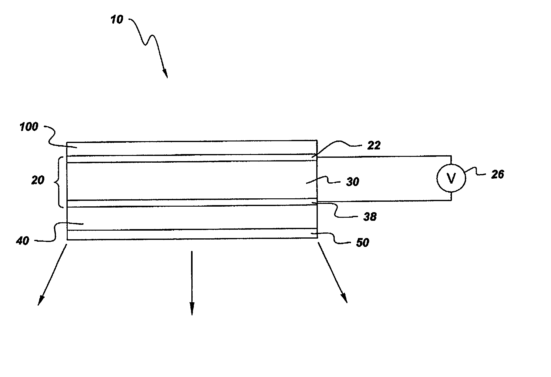
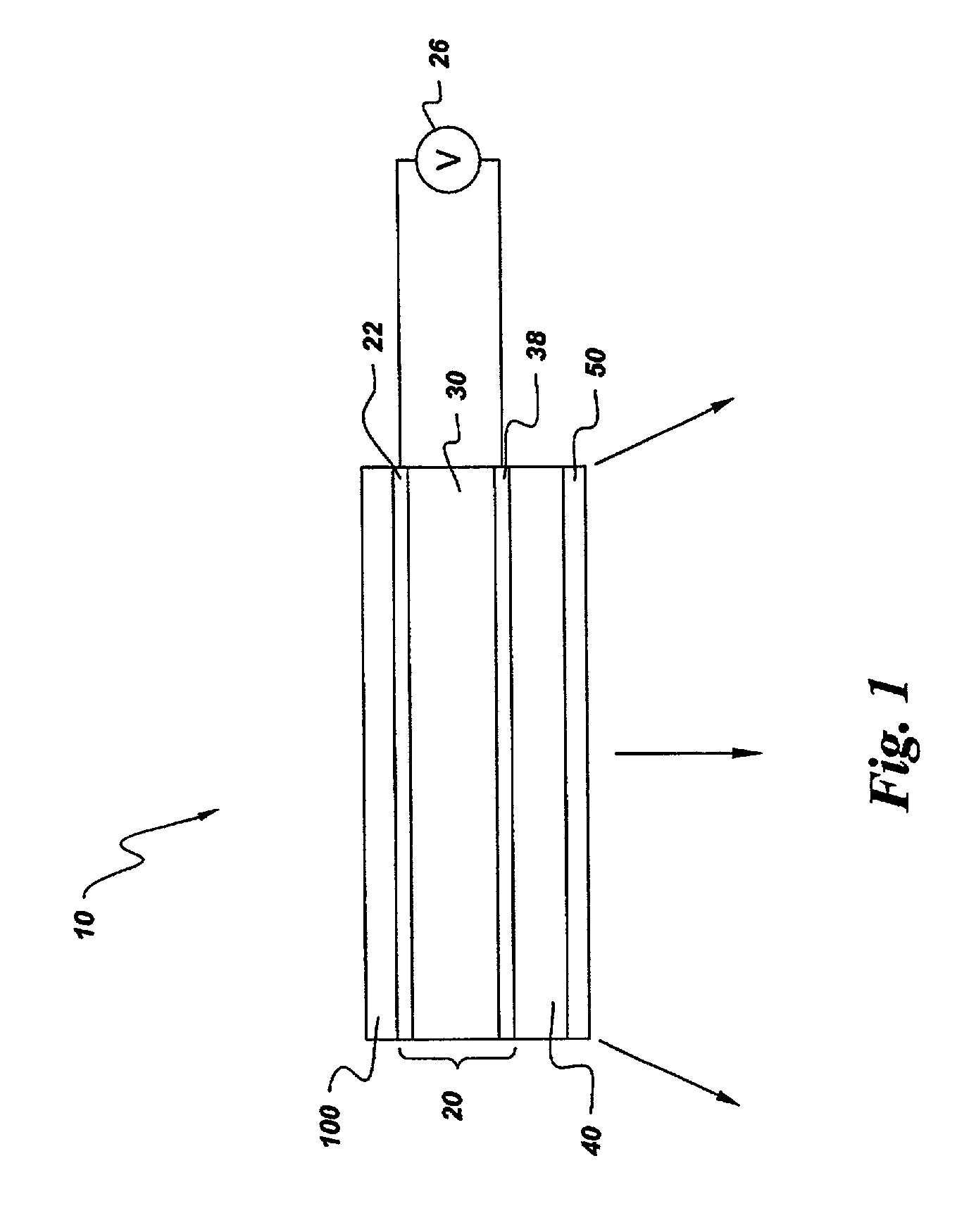
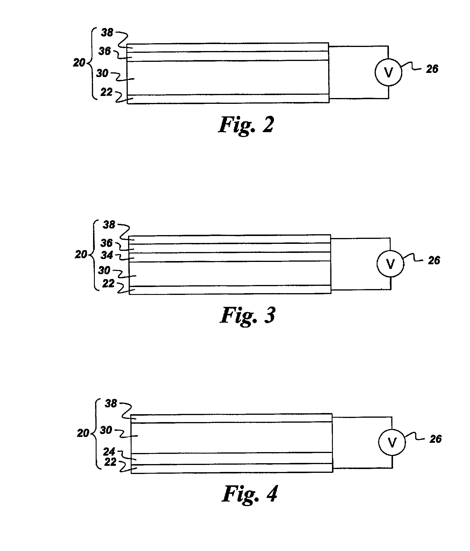
[0057] A light-emitting device of the present invention was constructed on a glass substrate having a dimension of about 5 cm.times.5 cm. It is understood that devices having larger areas may be made according the method disclosed herein. Soda lime glass substrates with a transparent, low resitivity (15 Ohms / square) ITO film on one side were obtained from Applied Films Corporation. The ITO was then patterned by use of standard photolithography techniques. Following a solvent clean and oxygen plasma treatment, a thin (60 nm) film of poly(3,4)-ethylenedioxythiophene / polyst-yrene sulfonate ("PEDOT / PSS") polymer was immediately deposited atop the ITO via spin casting. The PEDOT / PSS solution was obtained from Bayer AG of Germany under the name of Baytron P, and was used as received. The resulting film was baked under a nitrogen atmosphere for one hour at 200.degree. C. A blue light-emitting organic EL material obtained from Cambridge Display Technologies (Cambridge, England) was deposite...


PUM


Abstract

A light-emitting device comprises a light-emitting member, which comprises two electrodes and an organic electroluminescent material disposed between the electrodes, and at least one organic photoluminescent ("PL") material. The light-emitting member emits light having a first spectrum in response to a voltage applied across the two electrodes. The organic PL material absorbs a portion of the light emitted by the light-emitting member and emits light having second spectrum different than the first spectrum. The light-emitting device can include an inorganic PL material that absorbs another portion of the light emitted from the light-emitting member and emits light having a third spectrum different than both the first and the second spectra.

Description

BACKGROUND OF INVENTION[0002] The present invention relates generally to light-emitting devices having organic electroluminescent material and, more particularly, to light-emitting devices wherein light emitted from an organic electroluminescent layer is modified by organic and / or inorganic photoluminescent materials.[0003] Electroluminescent ("EL") devices, which may be classified as either organic or inorganic, are well known in graphic display and imaging art. EL devices have been produced in different shapes for many applications. Inorganic EL devices, however, typically suffer from a required high activation voltage and low brightness. On the other hand, organic EL devices ("OELDs"), which have been developed more recently, offer the benefits of lower activation voltage and higher brightness in addition to simple manufacture, and, thus, the promise of more widespread applications.[0004] An OELD is typically a thin film structure formed on a substrate such as glass or transparen...

Claims


Application Information

Patent Timeline
IPC IPC(8): H01L51/50H01L51/52H05B33/14
CPCH01L51/5036H05B33/14H01L51/5262H10K50/125H10K50/85
Inventor MCNULTY, THOMAS FRANCISDUGGAL, ANIL RAJTURNER, LARRY GENESHIANG, JOSEPH JOHN
Owner BOE TECH GRP CO LTD
Why Eureka
Try Eureka