Semiconductor device with selectively diffused regions

a technology of selective diffusion and semiconductors, applied in the direction of electrical equipment, climate sustainability, photovoltaic energy generation, etc., can solve the problems of increasing production costs, increasing complexity and manufacturing costs, and considerable efficiency losses

Inactive Publication Date: 2003-07-17
INTERUNIVERSITAIR MICRO ELECTRONICS CENT (IMEC VZW)
View PDF16 Cites 126 Cited by
  • Summary
  • Abstract
  • Description
  • Claims
  • Application Information

AI Technical Summary

Problems solved by technology

The formation of these differently doped regions often implies additional process steps that increase the cost of production.
The same diffusion region 7 over the whole front side combined with a low-cost metallisation technique such as screen printing of front metal contacts 4 leads to considerable efficiency losses.
This latter technique has the disadvantages of an extra masking and a difficult etching step which increase the complexity and cost of manufacture.
However, the selective emitter / collector structure requires a more complicated manufacturing process as described, for instance, in DE 42 17 428 in which a shallow emitter layer is diffused over the whole front surface of the substrate followed by the formation of passivation / oxide layers.

Method used


Image

  • Semiconductor device with selectively diffused regions
  • Semiconductor device with selectively diffused regions
  • Semiconductor device with selectively diffused regions

Examples


Embodiment Construction

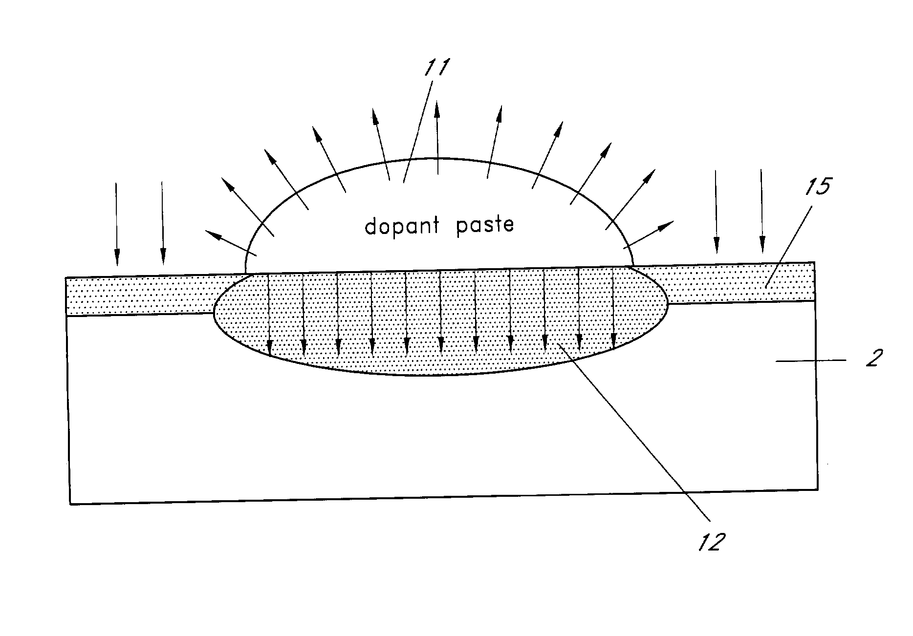
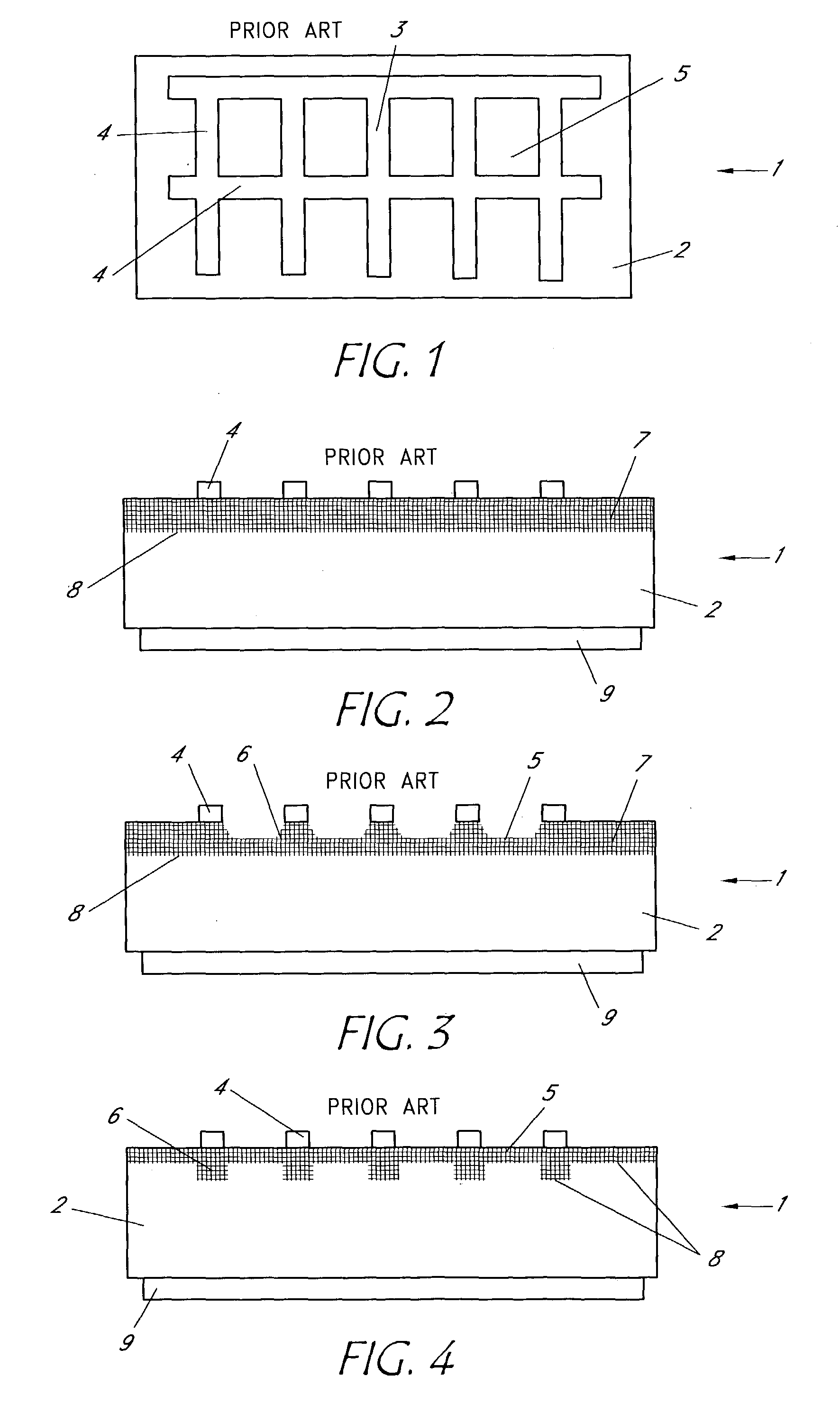
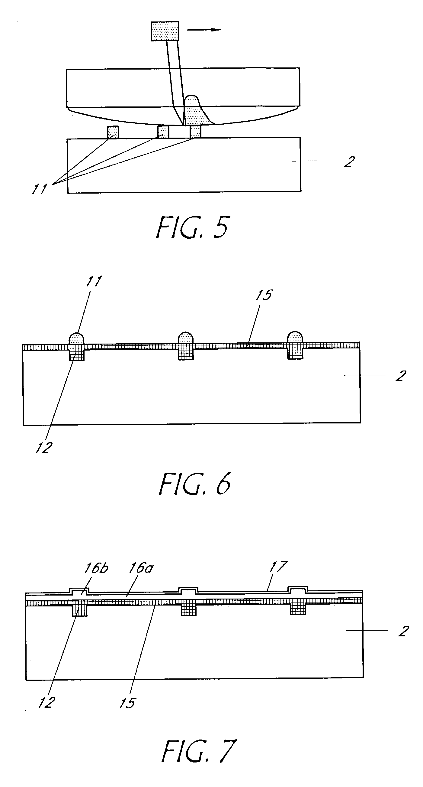
[0022] In the following the invention will be described with reference to certain specific embodiments and with reference to the drawings but the invention is not limited thereto but only by the claims. In the drawings some of the dimensions, for instance the thickness of layers, may have been exaggerated for purposes of clarity. In particular, the invention will be explained with reference to a photovoltaic device, sometimes called a solar cell, but the invention is not limited thereto but may find application in semiconductor devices generally. Further, the invention will mainly be described with reference to the formation of differentiated n++- and n+-type regions in a p-type substrate. The invention is not limited thereto. The methods of the present invention may be applied to the formation of differentiated p-type regions in an n-type substrate or the formation of n++-and n+-type regions in an undoped or n-type substrate or p++- and p+-type regions in an undoped or p-type subst...


PUM


Abstract

The present invention describes a method of manufacturing a semiconductor device, comprising a semiconductor substrate in the shape of a slice, the method comprising the steps of: step 1) selectively applying a pattern of a solids-based dopant source to a first major surface of said semiconducting substrate; step 2) diffusing the dopant atoms from said solids-based dopant source into said substrate by a controlled heat treatment step in a gaseous environment surrounding said semi-conducting substrate, the dopant from said solids-based dopant source diffusing directly into said substrate to form a first diffusion region and, at the same time, diffusing said dopant from said solids-based dopant source indirectly via said gaseous environment into said substrate to form a second diffusion region in at least some areas of said substrate to form a second diffusion region in at least some areas of said substrate not covered by said pattern; and step 3) forming a metal contact pattern substantially in alignment with said first diffusion region without having etched said second diffusion region substantially.

Description

[0001] The present invention relates to a semiconductng device and a method for the manufacture thereof, in particular to a photovoltaic cell having two or more selectively diffused regions produced in a single diffusion step.TECHNICAL BACKGROUND[0002] Many semiconductor devices make use of differently doped regions of the same conductivity type (p or n) to achieve better performance of the device. The formation of these differently doped regions often implies additional process steps that increase the cost of production. A typical semiconductor device 1 is shown in top-view in FIG. 1, which may be a photovoltaic cell, sometimes called a solar cell. A semiconductor substrate 2 of a first doping type has doped surface regions 5, typically of a second doping type, and a metallisation pattern 3 on at least one major surface. The metallisation pattern 3 usually includes elongate metal electrodes 4 between and under which are doped regions 5, e.g. emitter, collector or gate regions. The ...

Claims


Application Information

Patent Timeline
Patent Type & Authority Applications(United States)
IPC IPC(8): H01L21/00H01L31/0224H01L31/068H01L31/18
CPCH01L21/67109H01L21/67115H01L31/022425Y02E10/547H01L31/1804H01L31/0684H01L31/068Y02P70/50
Inventor HORZEL, JORGSZLUFCIK, JOZEFHONORE, MIANIJS, JOHAN
Owner INTERUNIVERSITAIR MICRO ELECTRONICS CENT (IMEC VZW)
Why Eureka
Try Eureka