Supporting gate contacts over source region on mosfet devices

a technology of mosfet devices and gate contacts, which is applied in the direction of semiconductor devices, semiconductor/solid-state device details, electrical apparatus, etc., can solve the problems of increasing the gate contact area in an attempt to ensure robustness, reducing the reliability of the parent device, and reducing the use of the parent device. , to achieve the effect of reliable, durable and economical

Inactive Publication Date: 2003-10-09
SEMICON COMPONENTS IND LLC
View PDF0 Cites 24 Cited by
  • Summary
  • Abstract
  • Description
  • Claims
  • Application Information

AI Technical Summary

Benefits of technology

0029] From the above descriptions, figures and narratives, the invention=s advantages in providing reliable, durable, and economical MOSFET gate contacts should be clear.

Problems solved by technology

A disadvantage of single gate bump contact designs is that mechanical and thermal stress experienced by this single gate bump contact can cause disconnection.
Inherent in multilayer metal stack technology, as commonly used in MOSFET contact areas, is the frequent problem of delamination of such metallization from its underlying dielectric layer due to differences between the coefficients of thermal expansion of the metallization and the dielectric when the stack is subjected to thermal stress.
Such delamination of the metallization renders the parent device inoperable and unusable.
Increasing the gate contact area in an attempt to guarantee robustness does not help, since the resulting contact still constitutes only a single connection.

Method used


Image

  • Supporting gate contacts over source region on mosfet devices
  • Supporting gate contacts over source region on mosfet devices
  • Supporting gate contacts over source region on mosfet devices

Examples


first embodiment

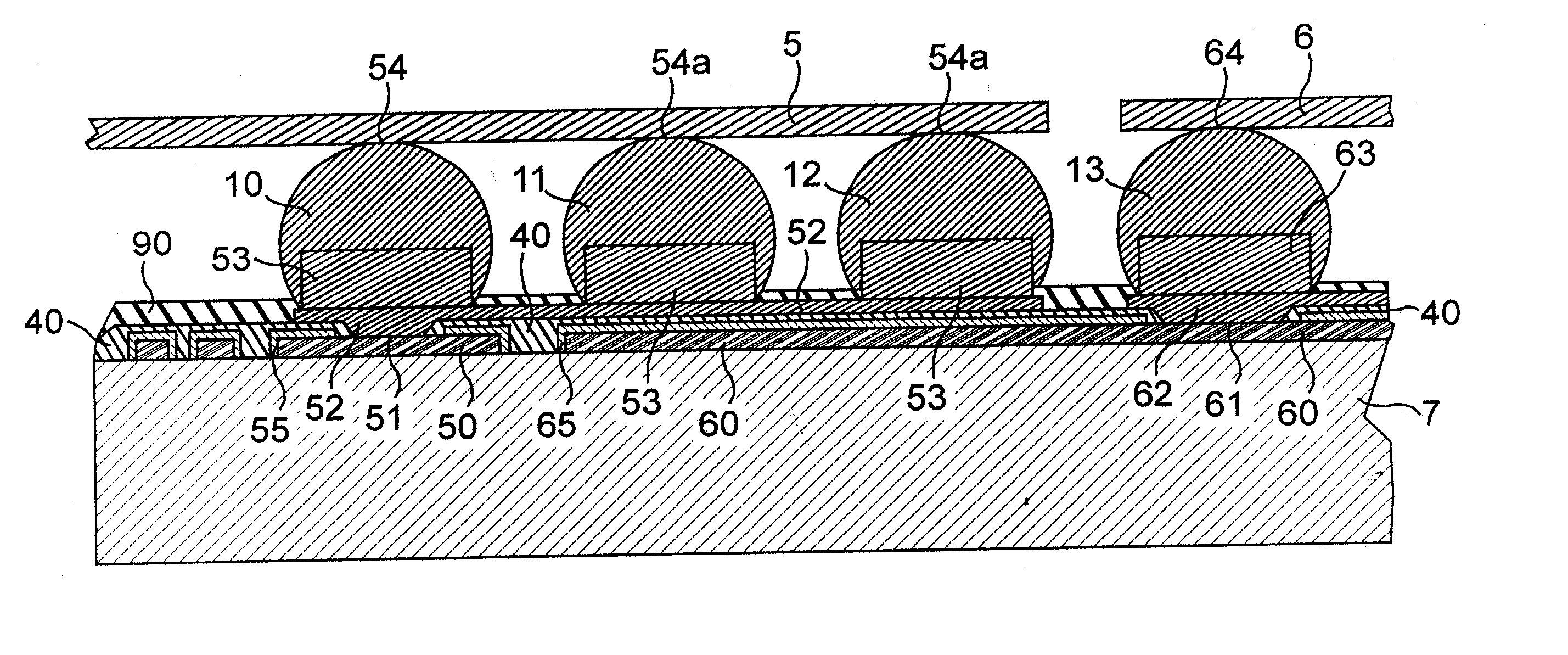
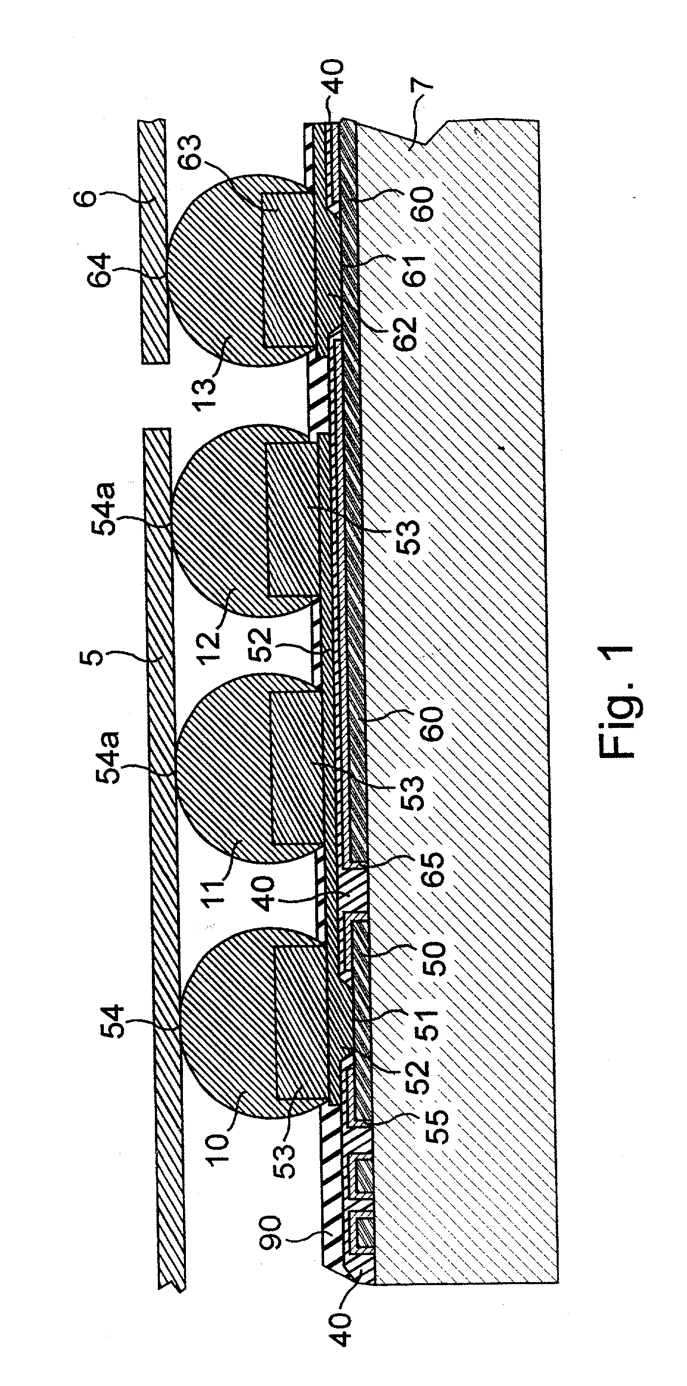
[0019] In a first embodiment, the invention adds one or more gate bump contacts by reallocating source bump contact locations to use as gate bump contacts. The added gate bump contacts provide both multiple electrical gate connections and multiple gate lead frame support points, at the cost of the loss of a few source bump contacts.

[0020] See FIG. 1, which shows a gate bump 10 and additional gate bumps 11, 12 connecting a gate contact 51 with package control gate connection 5, via gate bump contacts 54, 54a. FIG. 1 also shows one of a number of source bumps 13, connecting a source metallization 60, source contact 61, and source under bump metal 63, 63a with package source connection 6, via source bump contacts 64. The invention fabricates gate bump 10 directly over gate metallization 50, gate contact 51, and gate under bump metal 53, 53a, to make external gate bump contact 54 with package control gate connection 5. The invention also extends under bump metal 52 laterally over source...

second embodiment

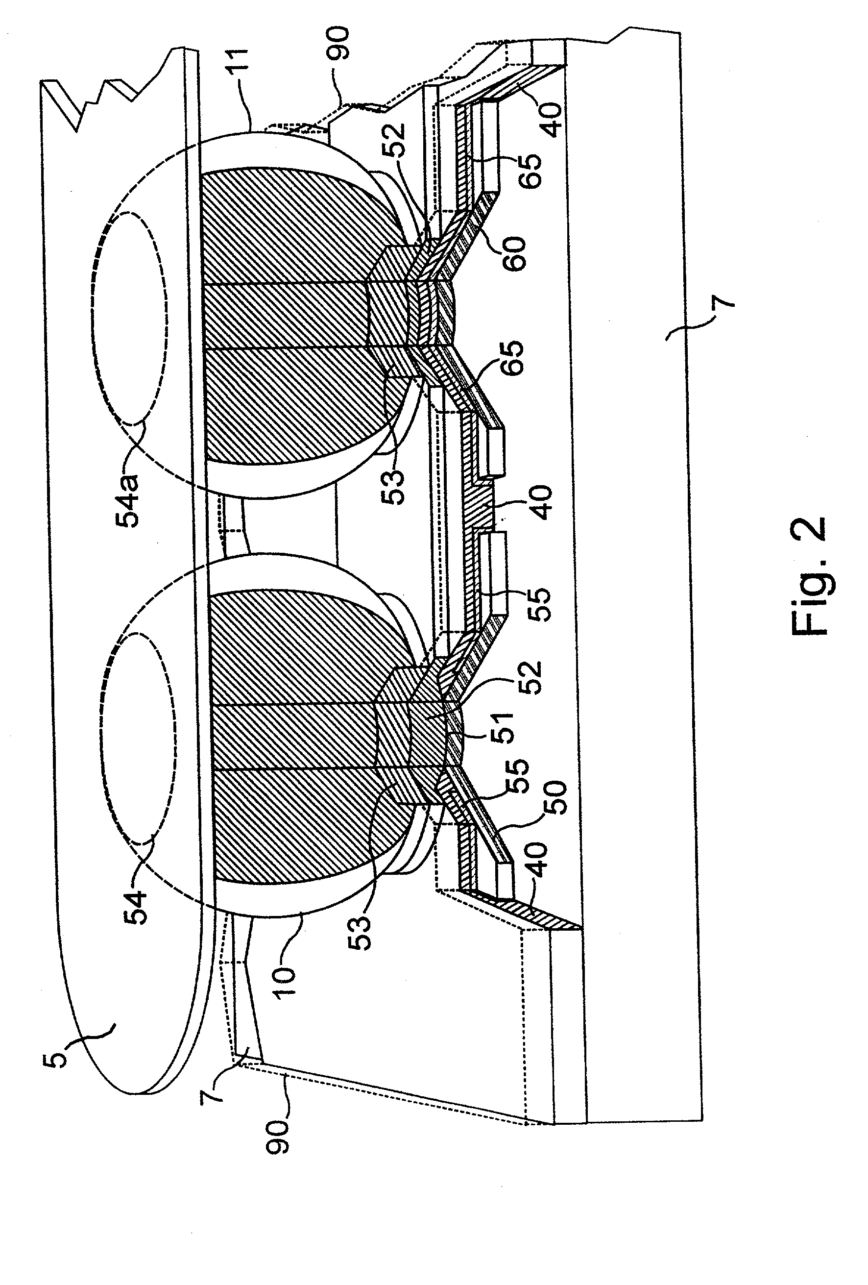
[0023] In a second embodiment, the invention eliminates the multilayer metal from atop the gate contact by laterally offsetting the gate bump contact and multi-metal layers from the gate contact region. This embodiment avoids multi-metal stacking on top of the gate metallization.

[0024] See FIG. 6, which shows two gate bumps 11, 12 connecting a gate contact 51 with package control gate connection 5, via gate bump contacts 54a. As in FIG. 1, FIG. 6 also shows one of a number of source bumps 13, connecting a source metallization 60, source contact 61, and source under bump metal 63 with package source connection 6, via source bump contacts 64. The invention fabricates gate under bump metal 52 directly over gate metallization 50 and gate contact 51, and extends under bump metal 52 laterally over source metallization 60, source passivation layer 65, and insulating layer 40 to connect gate contact 51 to gate bump contacts 11 and 12, and thus to gate bump contacts 54a over source metalliza...


PUM


Abstract

Increasing the number of MOSFET gate bump contacts makes MOSFET gate contacts more durable and reliable. Extension of the under-bump metal laterally from the gate contact with the gate pad metallization out to two or more gate pads overlying the source pad metallization reduces the risk of delamination of the metallization due to thermal and mechanical stresses in assembly and operation. Use of more than one gate pad further reduces such failure risks. The result is a reliable, durable MOSFET gate contact.

Description

[0001] This invention relates to semiconductor fabrication, and more specifically to power MOSFET contact fabrication.[0002] Definitions[0003] BCB: benzocyclobutene, an insulating polymer widely used as a photosensitive patterning material and insulator.[0004] RDSon: the on-state drain-to-source resistance in a MOSFET.[0005] UBM: under-bump metal, the conductive metal used to connect a source or gate contact to an external circuit via a surface solder bump.DISCUSSION OF PRIOR ART[0006] MOSFET die layouts are designed to maximize the source contact area for optimum RDSon performance. This approach leaves just enough area for the gate pad to establish one wirebonding connection or bump connection. With the increasing trend toward wireless packaging via wafer bumping and flipchip technologies, a single gate bump contact serves the purpose. A disadvantage of single gate bump contact designs is that mechanical and thermal stress experienced by this single gate bump contact can cause disc...

Claims


Application Information

Patent Timeline
Patent Type & Authority Applications(United States)
IPC IPC(8): H01L21/60H01L23/482H01L23/485
CPCH01L23/4824H01L24/11H01L2924/1306H01L2924/0001H01L2224/131H01L2924/014H01L2924/01033H01L2224/13099H01L2924/01013H01L2924/01015H01L2924/01022H01L2924/01029H01L2924/01078H01L2924/01082H01L2924/01327H01L2924/13091H01L24/13H01L2924/01005H01L2924/01006H01L2924/01019H01L2924/00H01L24/02H01L24/03H01L24/05H01L2224/05001H01L2224/05008H01L2224/05022H01L2224/05023H01L2224/05024H01L2224/05027H01L2224/05548H01L2224/05568H01L2224/05569H01L2224/13024H01L2224/1411H01L2924/351H01L2224/02
Inventor ESTACIO, MARIA CRISTINA B.BENDAL, R. EVAN
Owner SEMICON COMPONENTS IND LLC
Why Eureka
Try Eureka