Ink for forming a hole injection layer of organic EL display devices and manufacturing method thereof, organic EL display devices, and manufacturing method of the same

a technology of organic el and injection layer, which is applied in the direction of solid-state devices, discharge tubes/lamp details, natural mineral layered products, etc., can solve the problems of deterioration of display characteristics, generating display malfunction, and deterioration of the flatness of the film to be obtained

Inactive Publication Date: 2004-01-29
KK TOSHIBA
View PDF1 Cites 37 Cited by
  • Summary
  • Abstract
  • Description
  • Claims
  • Application Information

AI Technical Summary

Problems solved by technology

However, there is a problem that since this hole injection layer contains a low molecular weight solid component, this solid component is permitted to reach a polymeric luminescence layer due to the diffusion of the low molecular weight solid component as the EL element is actuated for a long period of time, thereby enabling the low molecular weight solid component to function as a trapping agent or a quencher, thus leading to the deterioration of the display characteristics.
Furthermore, since the ink containing this low molecular weight solid component is liable to flocculate, there are raised various p...

Method used


Image

  • Ink for forming a hole injection layer of organic EL display devices and manufacturing method thereof, organic EL display devices, and manufacturing method of the same
  • Ink for forming a hole injection layer of organic EL display devices and manufacturing method thereof, organic EL display devices, and manufacturing method of the same
  • Ink for forming a hole injection layer of organic EL display devices and manufacturing method thereof, organic EL display devices, and manufacturing method of the same

Examples


example

(III-4)

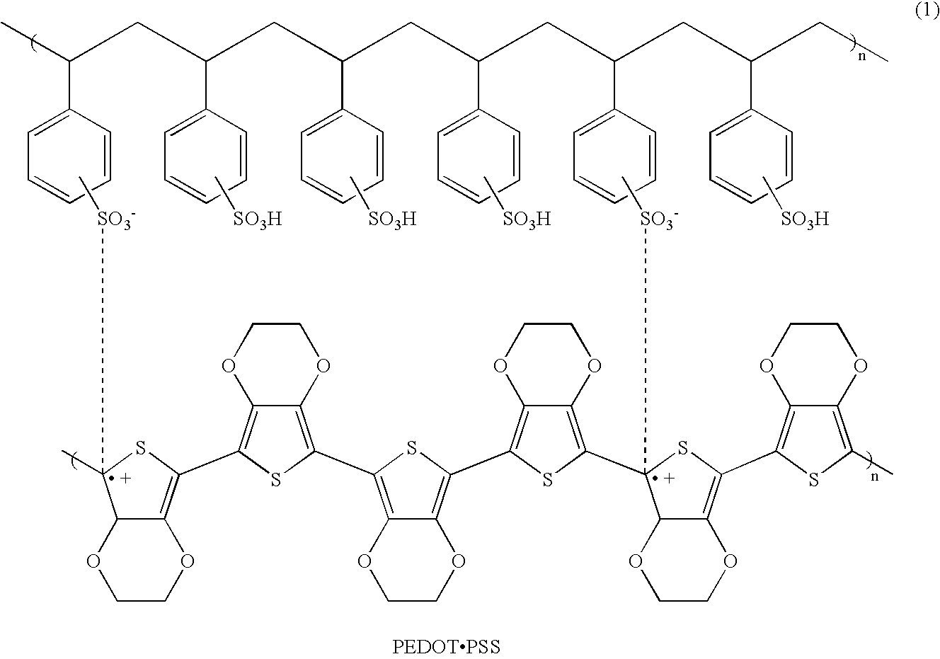
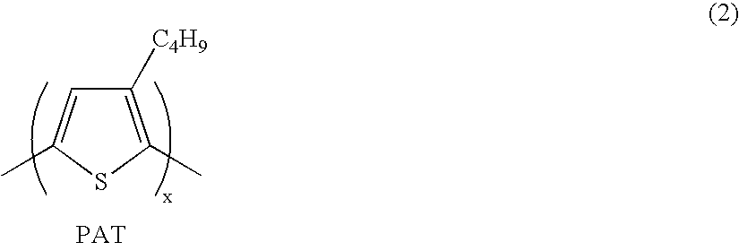
[0162] A trichromatic organic EL display device as shown in FIG. 1 was manufactured in the same manner as described in the aforementioned Example (III-2) except that the ink B4 shown in Table 7 was employed for forming the hole injection layers 5 and 6, and the ink D4 was employed for forming the hole injection layer 7.

[0163] When this organic EL display device was actuated at a current density of 20 mA / cm.sup.2, the half life in luminance of the display device was 12,000 hours.

[0164] As described above, according to the present invention, it is possible to provide an ink for forming a hole injection layer of organic EL display device, which makes it possible to manufacture an organic EL element which is excellent in hole injection property, can be hardly flocculated, and is long in useful life, to provide the manufacturing method thereof, to provide the method of manufacturing an organic EL display device having the aforementioned excellent features, and hence to provide suc...


PUM

PropertyMeasurementUnit
Fractionaaaaaaaaaa
Fractionaaaaaaaaaa
Fractionaaaaaaaaaa

Abstract

There is disclosed an organic electro luminescence display device comprising a two-dimensional array of pixels comprising organic electro luminescence elements capable of emitting a of color or different plural colors, each of the organic electro luminescence elements being provided with an anode, a cathode, a polymeric luminescence layer located between the anode and the cathode, and a hole injection layer. The hole injection layer is constituted by solid matters containing a donor molecule comprising polythiophene and/or a derivative thereof, and an acceptor molecule comprising polystyrenesulfonic acid and/or a derivative thereof, a concentration of sulfate ion in the hole injection layer is 125 ppm or less, and components having a molecular weight of 110,000 or less is 35% or less based on an entire solid matters, the molecular weight being converted as sodium polystyrenesulfonate in an aqueous gel permeation chromatography measured by using UV of 254 nm in wavelength.

Description

[0001] This application is based upon and claims the benefit of priority from the prior Japanese Patent Applications No. 2002-097913, filed Mar. 29, 2002; No. 2002-146561, filed May 21, 2002; and No. 2002-146562, filed May 21, 2002, the entire contents of all of which are incorporated herein by reference.[0002] 1. Field of the Invention[0003] The present invention relates to an ink for forming a hole injection layer of an organic EL (electro luminescence) display device, which makes it possible to manufacture an organic EL display device excellent in luminance and in long life, and to the method of preparing such an ink. The present invention also relates to a method of manufacturing an organic EL display device by using the aforementioned ink, and to the organic EL display device thus manufactured.[0004] 2. Description of the Related Art[0005] Recently, an electro luminescence (EL) element where a multi-layer film formed of an organic material is employed is attracting many attenti...

Claims


Application Information

Patent Timeline
IPC IPC(8): C09K11/06H01L27/32H01L51/00H01L51/30H01L51/40H01L51/50H05B33/14
CPCC09K11/06C09K2211/1029C09K2211/1425H01L27/3244H01L51/0005H01L51/0025Y10S428/917H01L51/0037H01L51/0038H01L51/0039H01L51/0062H01L51/5088H05B33/14H01L51/0036H10K59/12H10K71/135H10K71/311H10K85/113H10K85/115H10K85/1135H10K85/114H10K85/649H10K50/17H05B33/10
Inventor NAITO, KATSUYUKIKIHARA, NAOKOHASEGAWA, REIENOMOTO, SHINTARONAKAI, YUTAKAYAMAMOTO, KAZUSHIGEIWANAGA, HIROKISAKAI, KIMITOMORI, YASUSHI
Owner KK TOSHIBA
Why Eureka
Try Eureka