Analysis module, integrated circuit, system and method for testing an integrated circuit

Active Publication Date: 2004-04-01
NXP USA INC
View PDF9 Cites 2 Cited by
  • Summary
  • Abstract
  • Description
  • Claims
  • Application Information

AI Technical Summary

Problems solved by technology

A known problem with such arrangements is that the abovementioned physical parameters are not readily isolated and identified from within the integrated circuitry.
Particularly in the field of new and emergi

Method used


Image

  • Analysis module, integrated circuit, system and method for testing an integrated circuit
  • Analysis module, integrated circuit, system and method for testing an integrated circuit
  • Analysis module, integrated circuit, system and method for testing an integrated circuit

Examples


Embodiment Construction

)

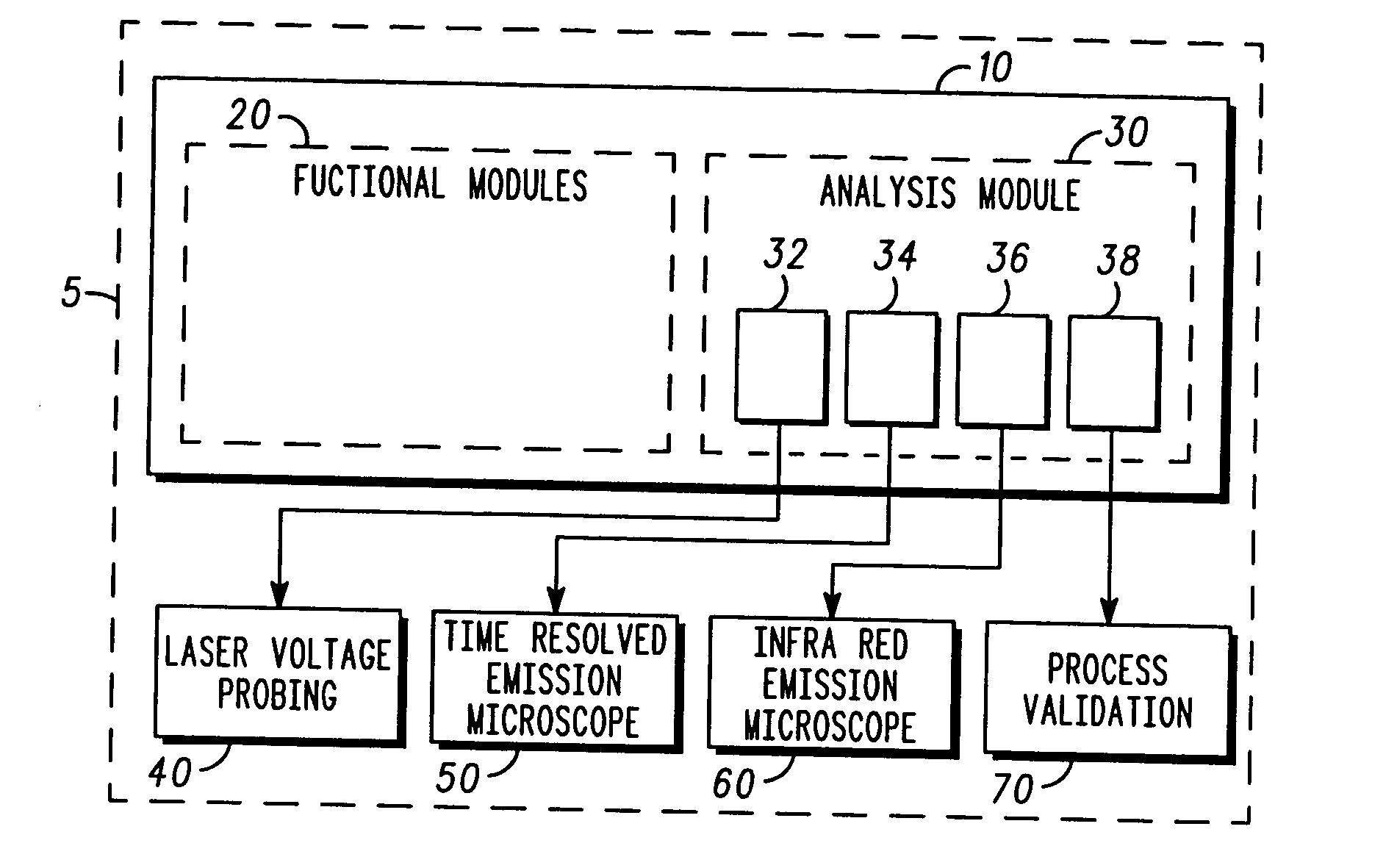
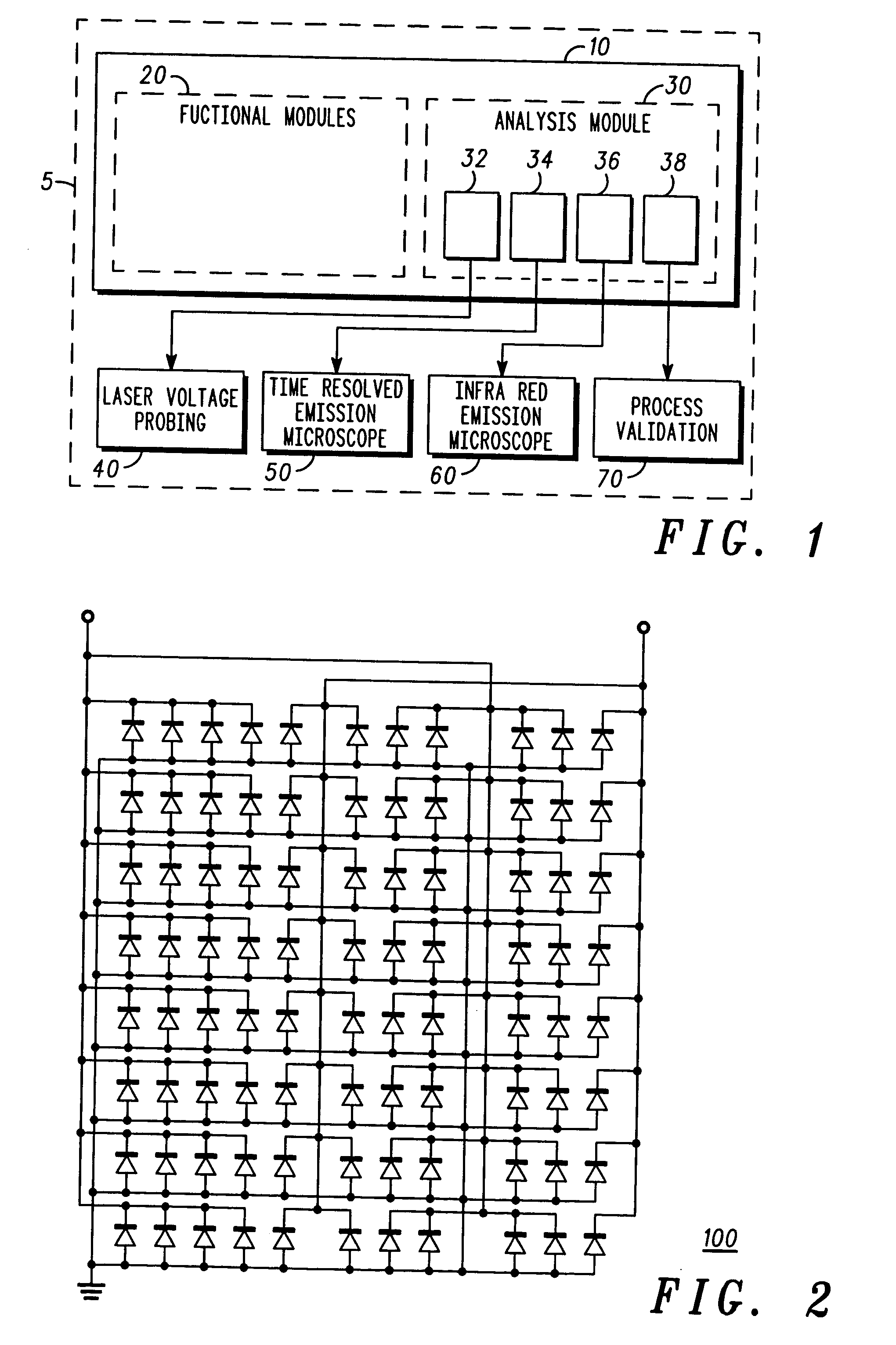
[0023] Failure Analysis (FA) instruments used for analysis of an Integrated Circuit (IC) die typically operate by taking measurements relating to the circuitry through the backside of the die. These measurements are then used to Locate the failure by measuring various physical aspects or parameters of the IC.

[0024] Referring to FIG. 1, there is a system 5 shown for testing an Integrated Circuit (IC) 10 according to the present invention. The system incorporates a number of FA instruments: as a laser voltage probing system 40, a Time Resolved Emission Microscope (TRLEM) 50 and an Infrared Emission Microscope (IREM) 60. The system also incorporates electrical characterization equipment 70.

[0025] The IC 10 includes a first semiconductor area comprising function modules 20 and a second semiconductor area comprising an analysis module 30. The analysis module 30 includes four submodules 32, 34 36 and 38 respectively, to be further described below. The function modules 20 are those elemen...


PUM


Abstract

A system (5) for testing and failure analysis of an integrated circuit (10) is provided using failure analysis tools (40, 50, 60). An analysis module (30) having a number of submodule test structures is incorporated into the integrated circuit design. The test structures are chosen in dependence upon the failure analysis tools (40, 50, 60) to be used. The rest of the integrated circuit contains function modules (20) arranged to provide normal operating functions. By analysing the submodule test structures of the analysis module (30) using the failure analysis tools (40, 50, 60), physical parameters of the integrated circuit (10) are obtained and used in subsequent testing of the function modules (20) by the failure analysis tools (40, 50, 60), thus simplifying the testing of the integrated circuit (10) and reducing the time taken to perform a failure analysis procedure.

Description

[0001] This invention relates to testing and failure analysis of Very Large Semiconductor Integrated circuit (VLSI) devices and particularly but not exclusively to testing of devices using failure analysis tools.[0002] The testing and failure analysis of integrated semiconductor devices is well known and a number of Failure Analysis (FA) tools have been developed. For example it is known from U.S. Pat. No. 5,760,892 to provide a method of analyzing failure of a semiconductor device using an emission microscope.[0003] It is also known from U.S. Pat. No. 6,153,891 to provide a method and apparatus providing a circuit edit structure through the backside of an integrated circuit die.[0004] It is also known from U.S. Pat. No. 5,294,812 to provide a semiconductor device having an identification region which may be inspected by eye in order to discern information about the device.[0005] Typically, such FA tools are used to measure and evaluate the performance of an integrated circuit are s...

Claims


Application Information

Patent Timeline
IPC IPC(8): G01R31/28G01R31/30G01R31/311H01L23/544
CPCG01R31/2884H01L22/34G01R31/311G01R31/30
Inventor WEIZMAN, YOAVSHPERBER, SHAIBARUCH, EZRA
Owner NXP USA INC
Why Eureka
Try Eureka