Device structure having enhanced surface adhesion and failure mode analysis

a surface adhesion and device structure technology, applied in semiconductor devices, semiconductor/solid-state device details, electrical devices, etc., can solve the problems of increasing the difficulty of failure mode analysis, difficult removal of ultra-low-k films, and insufficient adhesion between conductive materials and low dielectric constant materials for integrated circuit use, etc., to achieve the effect of improving failure mode analysis

Inactive Publication Date: 2007-01-02
TAIWAN SEMICON MFG CO LTD
View PDF4 Cites 2 Cited by
  • Summary
  • Abstract
  • Description
  • Claims
  • Application Information

AI Technical Summary

Benefits of technology

[0008]It is the object of this invention to provide a method for improving failure mode analysis.
[0009]It is another object of this invention to provide a method for easily removing a low dielectric constant dielectric material for failure mode analysis.
[0010]It is a further object of this invention to provide a method for easily removing a porous low dielectric constant dielectric material for failure mode analysis.
[0011]Yet another object is to provide an opening in a porous dielectric material having a conductor embedded in the opening wherein the interface between the dielectric and the conductor has roughness.

Problems solved by technology

This increases the difficulty of failure mode analysis since the metal cannot be removed by dry etching.
However, these ultra low-k films are difficult to remove using the current wet etch solution.
Also, as devices shrink to 90 nm or below and using ultra low dielectric constant material as the IMD layer, the adhesion between conductive materials and the low dielectric constant materials is not sufficient for integrated circuit usage.

Method used


Image

  • Device structure having enhanced surface adhesion and failure mode analysis
  • Device structure having enhanced surface adhesion and failure mode analysis
  • Device structure having enhanced surface adhesion and failure mode analysis

Examples


Embodiment Construction

of THE PREFERRED EMBODIMENTS

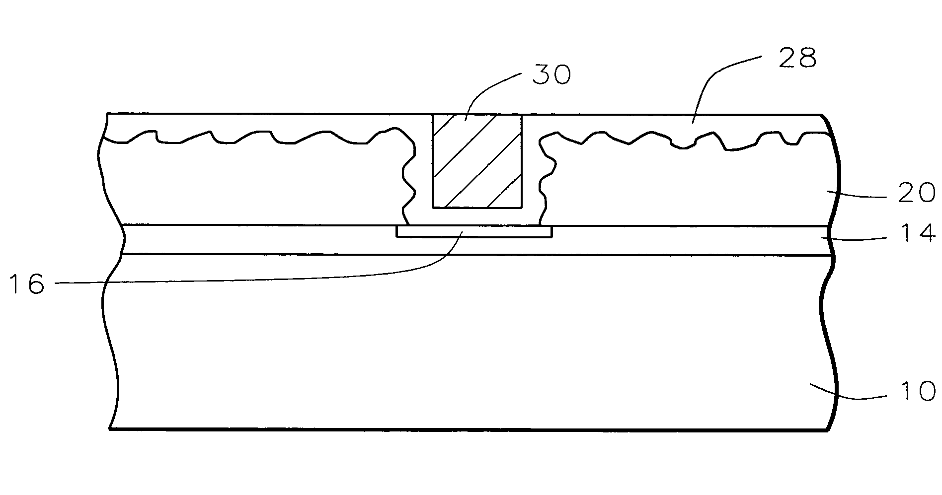
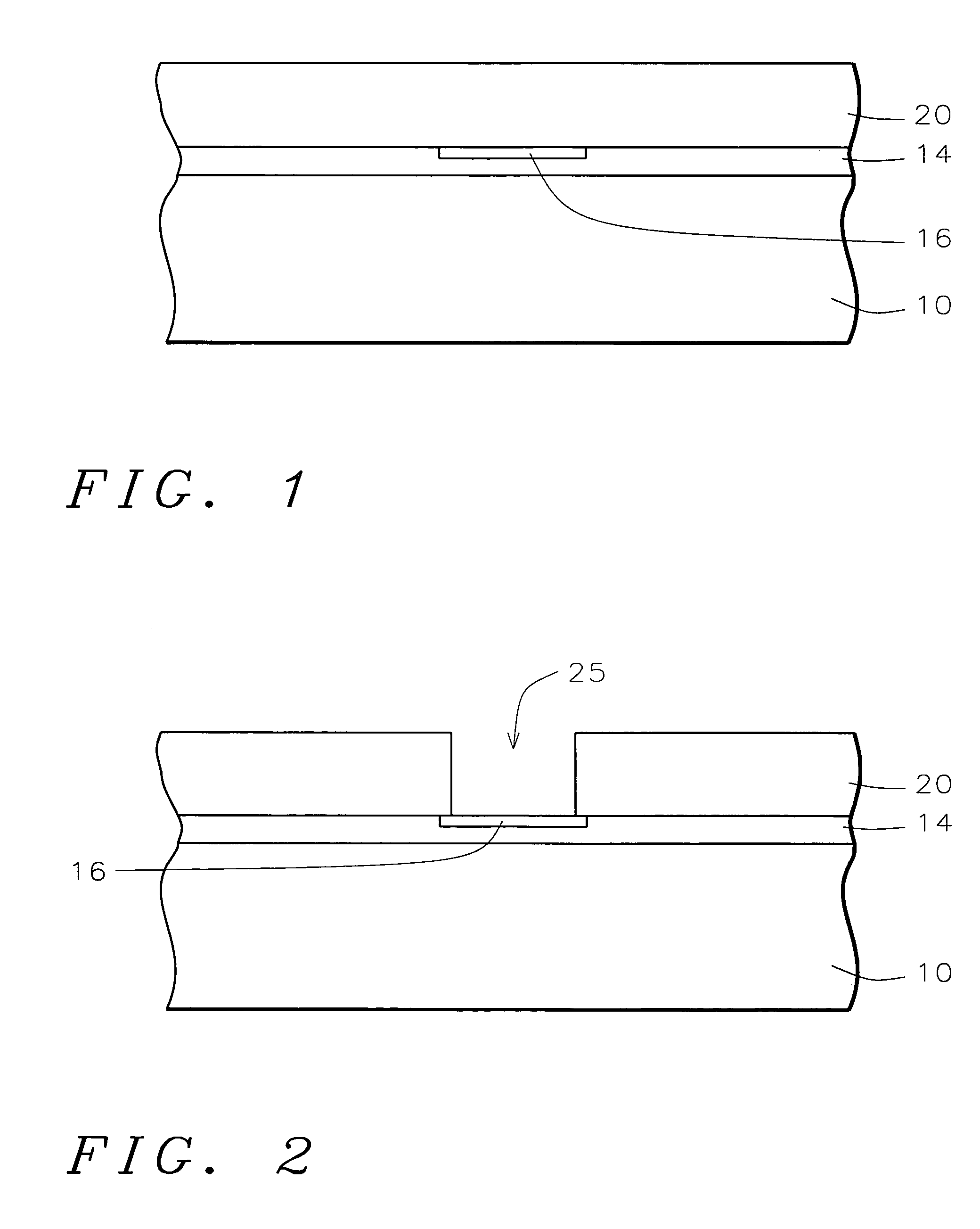
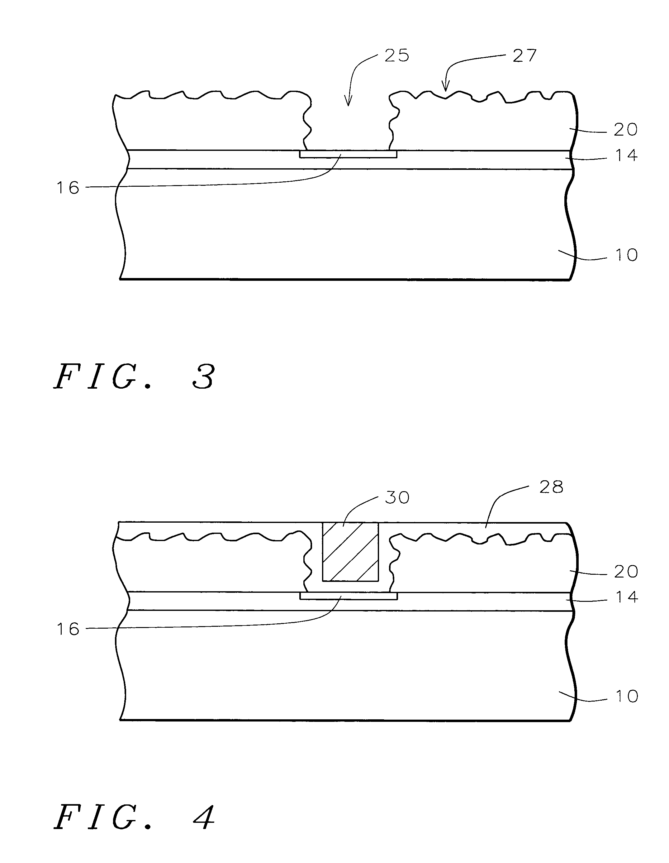
[0017]An enhanced surface adhesion between conductor layer and dielectric layer method is described with reference to FIGS. 1–4. An ultra low-k film containing a porogen is used. A new wet etch solution has been developed to remove this ultra low-k film or to roughen the surface of the ultra low-k film to provide a good adhesion.

[0018]Referring now to FIG. 1, there is illustrated a partially completed integrated circuit device. Semiconductor substrate 10 is illustrated. Semiconductor devices such as MOSFETs, not shown, are formed in and on the semiconductor substrate, as is conventional in the art. These devices are contained within the layer 14. Also within the layer 14 is a device 16 to be contacted by a copper line to be fabricated subsequently. An ultra-low dielectric constant material layer 20 is formed over the layer 14. The dielectric constant of the layer 20 will be less than 4.5, and preferably between 1.7 and 4.5. The dielectric material is sele...


PUM


Abstract

A substrate is provided having semiconductor device structures formed in and on the substrate. The semiconductor device structures comprise conductor layers embedded in openings in dielectric layers having a dielectric constant of less than 4.5. The dielectric layer has a roughness between the dielectric and the conductor wherein the roughness of the dielectric layer divided by the thickness of a barrier layer underlying the conductor layer is 0 to 1. The integrated circuit structure is prepared for failure analysis by removing the low dielectric constant dielectric layers and exposing the conductor layers for further failure analysis by optical examination or scanning electron microscope (SEM).

Description

BACKGROUND of the INVENTION[0001]1. Field of Invention[0002]This invention is directed to a method for failure mode analysis and more particularly to a method of removing a low dielectric constant material in preparation for failure mode analysis in the manufacture of integrated circuits.[0003]2. Description of Related Art[0004]In the manufacture of integrated circuits, failure mode analysis is an important tool for improving the manufacturing process. One important process is the fabrication of metal lines. In failure mode analysis of this process, it is necessary to check the surface of the metal film in order to check for voiding at the metal surface and it is also necessary to check the cross-section to check for voiding in the via hole. Copper damascene metallization has become very popular in integrated circuit fabrication. Copper is deposited within a damascene opening and then polished such as by chemical mechanical polishing (CMP) to leave the copper only within the opening...

Claims


Application Information

Patent Timeline
Patent Type & Authority Patents(United States)
IPC IPC(8): H01L21/4763H01L21/44H01L21/768
CPCH01L21/76802H01L2924/0002H01L2924/00
Inventor LIN, HWAY CHICHENG, YI-LUNGWANG, CHAO-HSIUNG
Owner TAIWAN SEMICON MFG CO LTD
Why Eureka
Try Eureka