Method and apparatus for picking up a semiconductor chip, method and apparatus for removing a semiconductor chip from a dicing tape, and a method of forming a perforated dicing tape

a technology of dicing tape and semiconductor chip, which is applied in the direction of electrical apparatus, conveyor parts, semiconductor devices, etc., can solve the problems of increasing manufacturing costs, chip damage, and severe damage to thin chips, and affecting the quality of semiconductor chips

Inactive Publication Date: 2004-05-13
SAMSUNG ELECTRONICS CO LTD
View PDF9 Cites 42 Cited by
  • Summary
  • Abstract
  • Description
  • Claims
  • Application Information

AI Technical Summary

Problems solved by technology

However, because the needle applies physical stress to the semiconductor chip, the needle may damage the chip as it forcibly pushes the semiconductor chip off the dicing tape.
In addition, because semiconductor chip thickness has been reduced so that thin semiconductor packages that have a thickness of several tens of .mu.m or multi chip packages that have a thickness of several hundred .mu.m or less may be formed, the conventional needle pick-up method may cause severe damage to such a thin chip.
Because a damaged semiconductor chip 30 is not easily separated from the dicing tape 10 and leads to defective units, manufacturing costs may be increased.
The blown air may create a space between the semiconductor chip and the dicing tape, which may weaken the adhesion of the dicing tape to the semiconductor chip.

Method used


Image

  • Method and apparatus for picking up a semiconductor chip, method and apparatus for removing a semiconductor chip from a dicing tape, and a method of forming a perforated dicing tape
  • Method and apparatus for picking up a semiconductor chip, method and apparatus for removing a semiconductor chip from a dicing tape, and a method of forming a perforated dicing tape
  • Method and apparatus for picking up a semiconductor chip, method and apparatus for removing a semiconductor chip from a dicing tape, and a method of forming a perforated dicing tape

Examples


Embodiment Construction

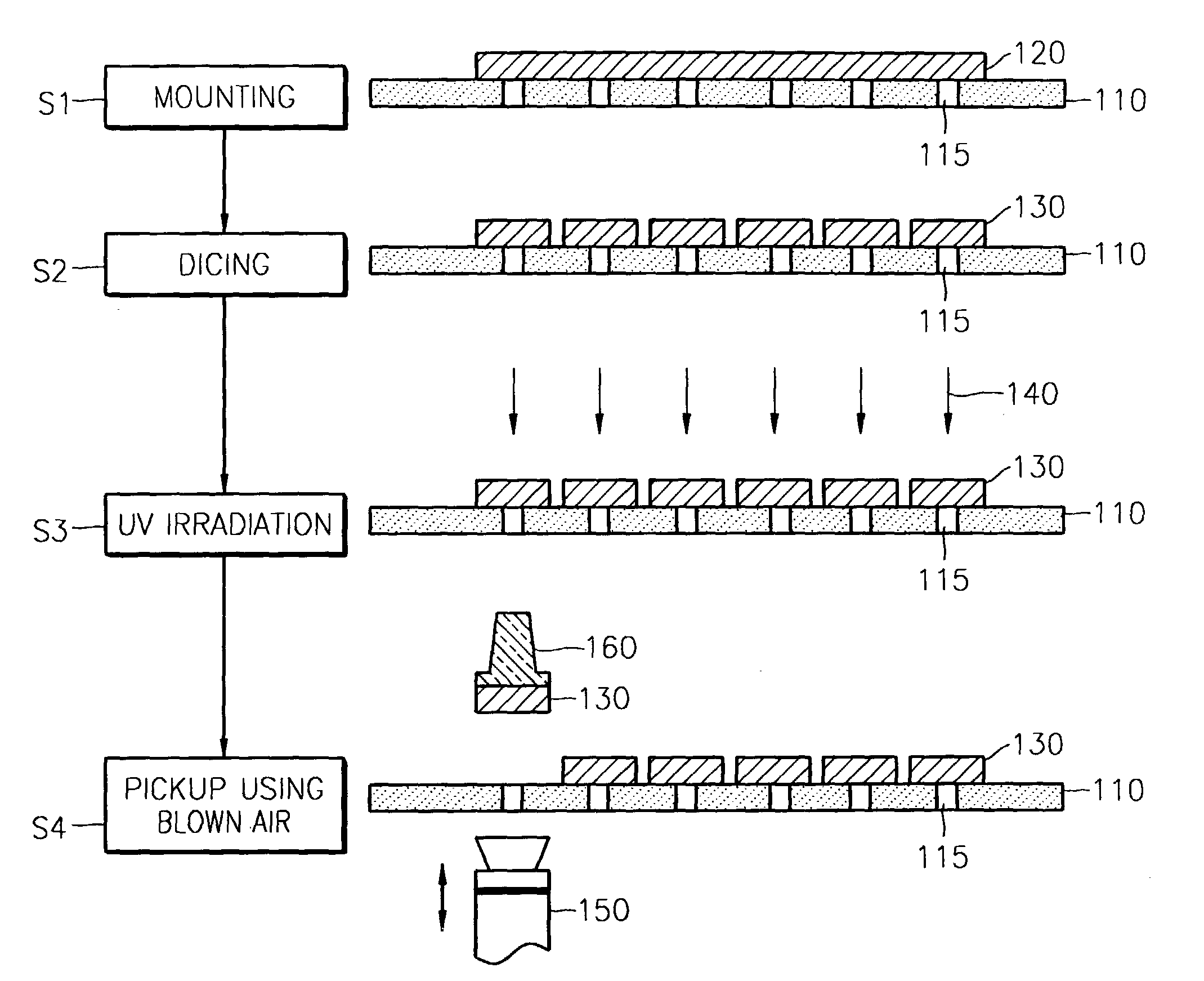
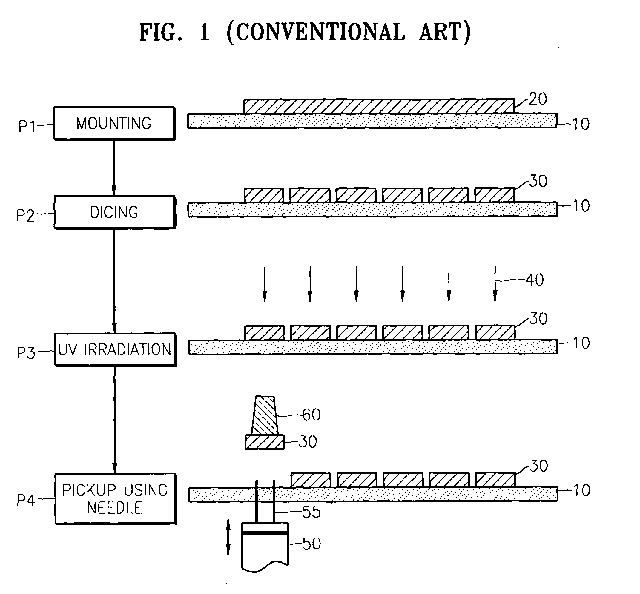
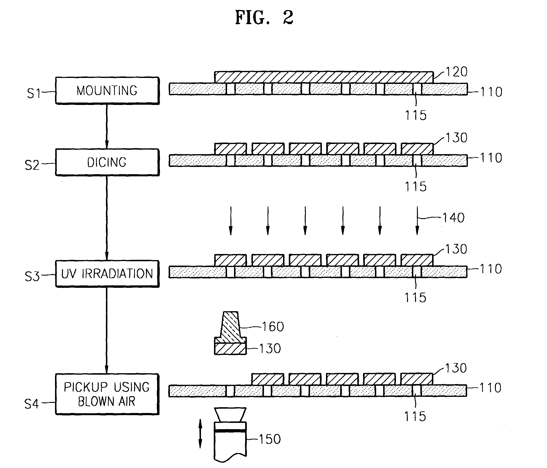
[0018] Exemplary embodiments of the present invention will now be described more fully with reference to the accompanying drawings, in which exemplary embodiments of the invention are shown. This invention may, however, be embodied in many different forms and should not be construed as being limited to the exemplary embodiments set forth herein. Rather, these exemplary embodiments are provided so that this disclosure will be thorough and complete and will fully convey the concept of the invention to those skilled in the art. In the drawings, the thicknesses of the layers and regions are exaggerated for clarity. Thus, the present invention should not be limited to the relative sizes or intervals shown in the appended drawings. It will also be understood that when an element is referred to as being "on" another element, it may be located directly on the other element or intervening elements may be present. It is to be further understood that when an element is referred to as being "un...


PUM


Abstract

A method and apparatus for picking up a semiconductor chip, a method and apparatus for removing a semiconductor chip from a dicing tape, and a method of forming a perforated dicing tape are provided. Air may be blown through air holes in a dicing tape to at least partially separate the semiconductor chip from the dicing tape and/or create a space between the semiconductor chip to weaken the adhesion of the dicing tape to the semiconductor chip. The semiconductor chip may then be picked up by a removal member and completely removed from the dicing tape. Semiconductor chips that are not to be removed may be vacuum-suctioned to the dicing tape. UV radiation or heat may be applied to weaken the adhesion of the dicing tape. The semiconductor chip may be detected by an optical detector. Removing the semiconductor chips by air reduces stress and damage to the semiconductor chips.

Description

[0001] This U.S. non-provisional application claims priority under 35 U.S.C. .sctn.119 to Korean Patent Application No. 2002-69666, filed on Nov. 11, 2002 in the Korean Intellectual Property Office, the contents of which are incorporated herein by reference in their entirety.[0002] 1. Field of the Invention[0003] The present invention relates generally to semiconductor assembly processes, and more particularly, to a method and apparatus for picking up a semiconductor chip by blowing air through air holes in a dicing tape to separate the semiconductor chip from the dicing tape and then picking up the semiconductor chip. A method of removing a semiconductor chip from a dicing tape and a method for forming a perforated dicing tape are also provided.[0004] 2. Description of the Related Art[0005] In semiconductor assembly processes, dividing a wafer into semiconductor chips may be termed "sawing" or "dicing." After the wafer has been diced or sawed into individual semiconductor chips, ea...

Claims


Application Information

Patent Timeline
Patent Type & Authority Applications(United States)
IPC IPC(8): H01L21/50H01L21/00H01L21/68
CPCH01L21/67132H01L21/6835H01L2221/68327H01L2221/68322H01L21/6836H01L21/50
Inventor YOO, CHEOL-JOON
Owner SAMSUNG ELECTRONICS CO LTD
Why Eureka
Try Eureka