Lid for use in packaging an electronic device and method of manufacturing the lid

a technology for electronic devices and lids, which is applied in the direction of device details, electrical apparatus casings/cabinets/drawers, and hermetically sealed casings. it can solve the problems of large time required for shaping operations, high cost of dies required to form ceramics into boxes, and side walls of the base can interfere with the installation of electronic devices on the bottom surface of the bas

Active Publication Date: 2004-05-20
SENJU METAL IND CO LTD
View PDF5 Cites 14 Cited by
  • Summary
  • Abstract
  • Description
  • Claims
  • Application Information

AI Technical Summary

Problems solved by technology

Since the base is box-shaped having side walls, the side walls of the base can interfere with the installation of the electronic device on the bottom surface of the base.
Furthermore, the dies required to form a ceramic into the shape of a box are expensive, and a great amount of time is required for shaping operations.
This portion of the base does not in any way contribute to the function of the electronic part, so it makes the electronic part unnecessarily large and it interferes with reduction in size of electronic equipment.

Method used


Image

  • Lid for use in packaging an electronic device and method of manufacturing the lid
  • Lid for use in packaging an electronic device and method of manufacturing the lid
  • Lid for use in packaging an electronic device and method of manufacturing the lid

Examples


example

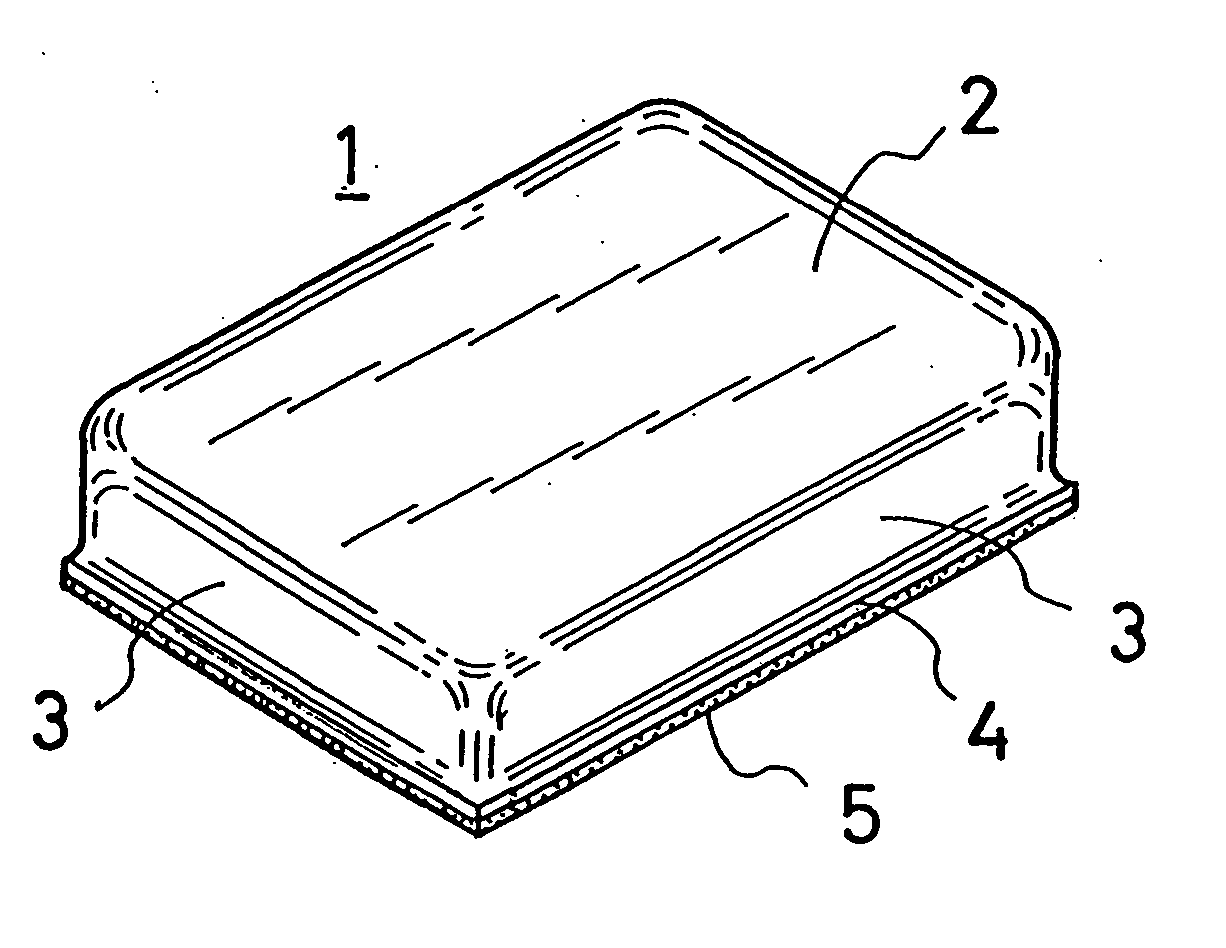
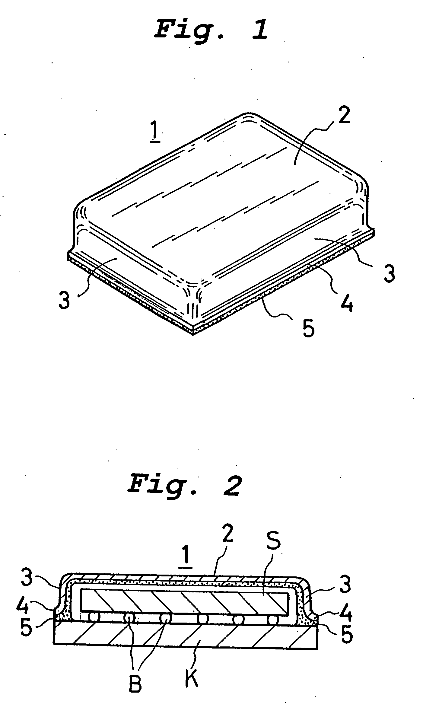
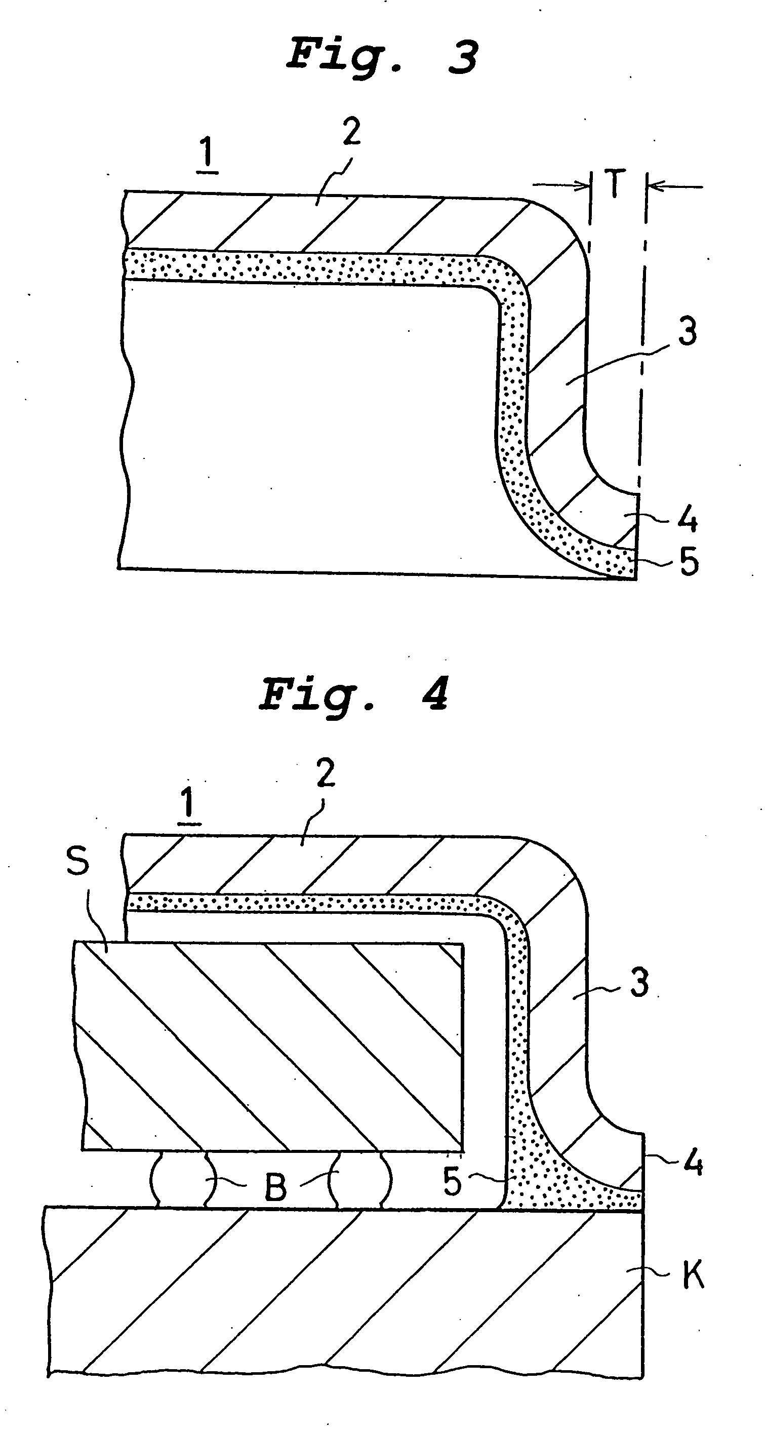
[0049] To demonstrate the effectiveness of a lid according to the present invention, a Pb-rich high temperature solder was applied by a molten solder method on one side of a Kovar strip having a thickness of 100 .mu.m to form a plated solder layer with a thickness of 20 .mu.m. The solder-plated strip was then subjected to drawing in the manner shown in FIG. 5B with a series of dies to form recessed shapes each having a rectangular top portion measuring 2.4.times.1.9 mm and having a depth of 0.4 mm. The solder layer is on the interior of the recessed shapes. The recessed shapes were then punched out of the strip with a punching press in the manner shown in FIG. 5C to obtain lids having a lip at the lower ends of the side walls of the lid and projecting from the outer surfaces of the side walls by 100 .mu.m.

[0050] One of the resulting lids was disposed on a plate-shaped base having the same outer contour as the lid and an Au layer on the top surface along its periphery with a width of...


PUM


Abstract

A lid for use with a plate-shaped base to seal an electronic device such as a SAW device includes a top portion, a wall structure extending from the top portion, and a lip connected to the lower end of the wall structure. The lip extends outwards from an outer surface of the wall structure by 10-500 mum and has solder on an inner surface thereof. The lid can be soldered to a plate-shaped base to form a package. The lid can be conveniently formed by performing drawing of a metal strip coated with solder to define a recessed shape, and then severing a flange of the recessed shape to define the lip.

Description

[0001] 1. Field of the Invention[0002] This invention relates to a lid for use in packaging an electronic device, and in particular to a cap-shaped lid which is suitable for use with a plate-shaped base and which has a solder layer on its inner surface. The present invention also relates to a method of manufacturing such a lid.[0003] 2. Description of the Related Art[0004] Minute electronic parts such as SAW (surface acoustic wave) filters are generally in the form of package which comprises a box-shaped ceramic base receiving an electronic device such as a surface acoustic wave device and a plate-shaped lid sealed to the top end surface of the box-shaped base. The lid is typically made of a material such as Kovar (a Co--Ni--Fe alloy) or Alloy 42 (42 Ni--Fe), which has a coefficient of thermal expansion close to that of a ceramic. A solder layer is formed on one side of the lid, and a layer of Au or other material which is easily wet by molten solder is provided on the top end surfa...

Claims


Application Information

Patent Timeline
Patent Type & Authority Applications(United States)
IPC IPC(8): H01L23/02H01J5/00H01L23/04H01L23/10H01L23/28H01L41/02H03H9/02H03H9/10
CPCH01L23/04H01L23/10H01L2224/16H01L2924/01078H01L2924/01019H01L2924/16152H01L2924/1617H03H9/1071H01L2924/01079H01L2924/00014H01L2224/0401H01L23/28
Inventor GOTO, MASAAKINISHIUCHI, FUMIAKINAKAJIMA, MISAOZEN, MITSUOTANIGUCHI, SANAEAZUMA, TAKENORI
Owner SENJU METAL IND CO LTD
Why Eureka
Try Eureka