AGC circuit
- Summary
- Abstract
- Description
- Claims
- Application Information
AI Technical Summary
Benefits of technology
Problems solved by technology
Method used
Image

Examples
first embodiment
[0065] (First embodiment)
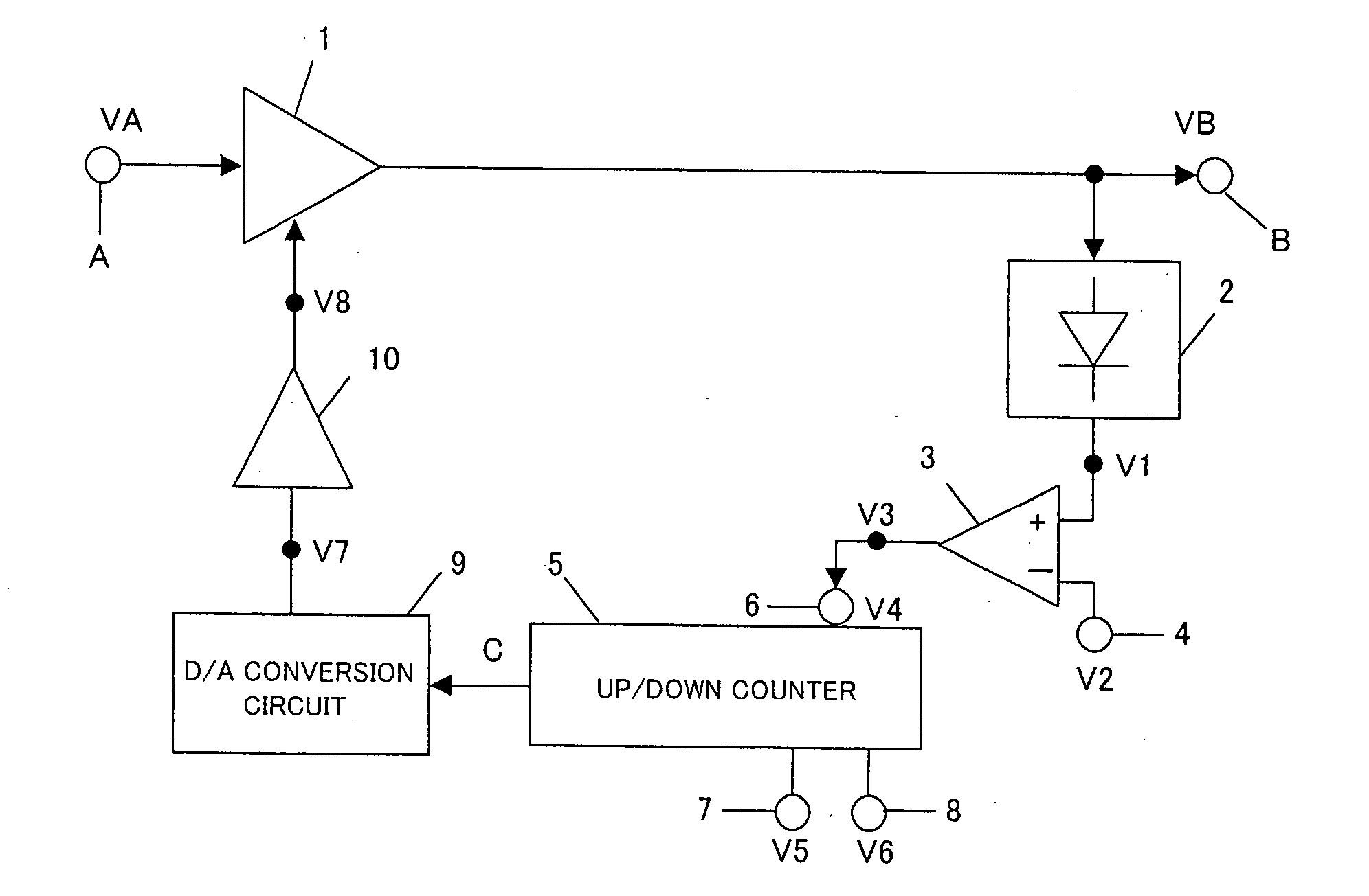
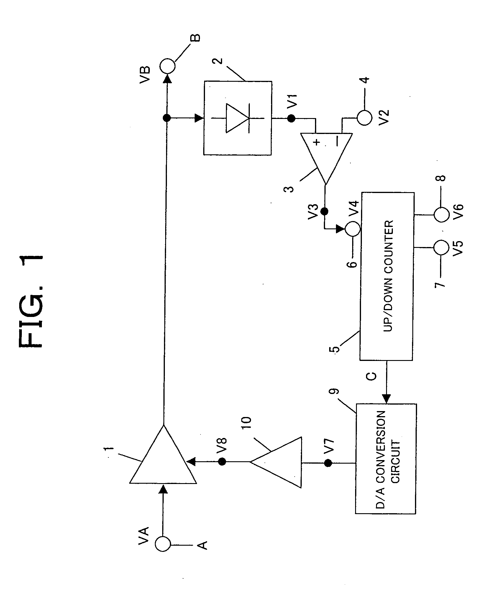
[0066] FIG. 1 is a block diagram showing the configuration of an AGC circuit according to a first embodiment of the invention. In FIG. 1, reference symbol A denotes a signal input terminal supplied with input signal VA. Reference numeral 1 denotes a variable gain amplifier circuit that amplifies or attenuates a voltage of input signal VA in accordance with a gain controlled by a gain control voltage V8 to output an output signal VB. Reference symbol B denotes an output terminal of the variable gain amplifier circuit 1. Reference numeral 2 denotes a rectification circuit that rectifies the output voltage of the variable gain amplifier circuit 1. Hereinafter, the rectification circuit 2 will be described as a full wave rectification circuit. However, a half wave rectification circuit is also applicable.
[0067] Reference numeral 3 denotes a first voltage comparator that compares rectified signal (output signal) V1 rectified by the rectification circuit 2 with a ...
second embodiment
[0086] (Second embodiment)
[0087] FIG. 4 is a block diagram showing the configuration of an AGC circuit of a second embodiment of the invention. In FIG. 4, the constituent elements, which are the same as those in the AGC circuit according to the first embodiment of the invention shown in FIG. 1, will given with the same reference numerals and symbols, and the description thereof will be omitted, and only the elements, which is newly added to the AGC circuit shown in FIG. 1, will be described.
[0088] Reference numeral 11 denotes a flip-flop as a register interposed between the first voltage comparator 3 and the up / down operation control input terminal 6 of the up / down counter 5. The flip-flop 11 stores polarity, i.e., voltage level (high level or low level) of a signal output from the first voltage comparator 3 at a cycle of the reference clock V9, and further transmits the polarity stored at the cycle of the reference clock V9 to the up / down operation control input terminal 6 of the f...
third embodiment
[0092] (Third embodiment)
[0093] FIG. 6 is a block diagram showing the configuration of an AGC circuit of a third embodiment of the invention. In FIG. 6, the constituent elements, which are the same as those in the AGC circuit according to the first embodiment of the invention shown in FIG. 1, will given with the same reference numerals and symbols, and the description thereof will be omitted. Only the elements, which are newly added to the AGC circuit shown in FIG. 1, will be described.
[0094] Reference numeral 13 denotes a first count operation control circuit that controls whether to transmit high level or low level voltage V3, which is output from the first voltage comparator 3, to the up / down operation control input terminal 6 or to shut down the transmission of the high level or low level voltage V3 in accordance with the count value C counted by the first up / down counter 5.
[0095] To be more precise, when the count value C is smaller than a predetermined upper limit value, the f...
PUM
 Abstract
Description
Claims
Application Information
 - Generate Ideas
- Intellectual Property
- Life Sciences
- Materials
- Tech Scout
- Unparalleled Data Quality
- Higher Quality Content
- 60% Fewer Hallucinations
Browse by: Latest US Patents, China's latest patents, Technical Efficacy Thesaurus, Application Domain, Technology Topic, Popular Technical Reports.
© 2025 PatSnap. All rights reserved.Legal|Privacy policy|Modern Slavery Act Transparency Statement|Sitemap|About US| Contact US: help@patsnap.com