III-nitride optoelectronic device structure with high Al AlGaN diffusion barrier

a technology of iii-nitride and electronic devices, applied in the direction of basic electric elements, semiconductor devices, electrical apparatus, etc., can solve the problems of reducing the efficiency of the product device, reducing the luminous efficiency of the device, and severely affecting the ultimate performance and efficiency of the iii-nitride optoelectronic device. , to achieve the effect of suppressing migration or diffusion

Active Publication Date: 2004-11-11
CREELED INC
View PDF8 Cites 37 Cited by
  • Summary
  • Abstract
  • Description
  • Claims
  • Application Information

AI Technical Summary

Benefits of technology

0012] Yet another aspect of the invention relates to a method of forming a III-nitride optoelectronic device structure including an active region and a doped III-nitride layer overlying the active region, such method comprising forming an AlGaN layer intermediate the active region and doped III-nitride layer, to form a barrier layer for suppressing migration or diffusion of dopant from the doped III-nitride layer into the active region.

Problems solved by technology

Such transport of the dopant species into the active region is severely detrimental to the ultimate performance and efficiency of the III-nitride optoelectronic device.
Specifically, the transport of dopant species into the active region of the optoelectronic device will reduce the luminous efficiency of the device due to formation of non-radiative centers, as well as radiative centers with undesirable wavelength characteristics (i.e., deviations from the desired emission wavelength), and the development of micro-morphological defects, which in turn substantially reduce the efficiency of the product device.
Further, such transport of dopant species into the active region, and the defects that resultantly develop in the device, lead to shortened product life, as a consequence of excessive heat generation during operation, attributable to the presence of dopant contamination of the active region.

Method used


Image

  • III-nitride optoelectronic device structure with high Al AlGaN diffusion barrier
  • III-nitride optoelectronic device structure with high Al AlGaN diffusion barrier
  • III-nitride optoelectronic device structure with high Al AlGaN diffusion barrier

Examples


example 1

[0067] The following provides a specific example of growth conditions for a UV LED device fabricated in accordance with the present invention.

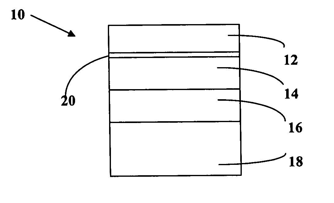
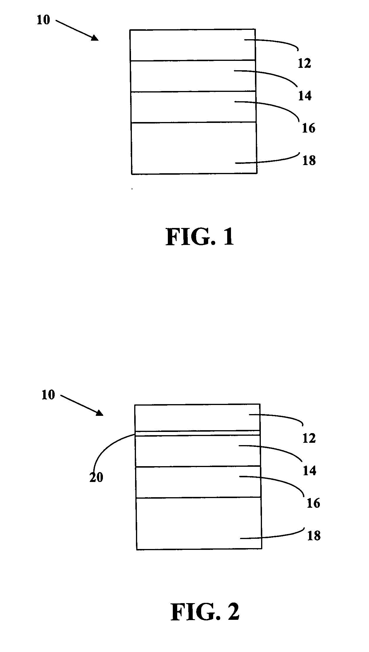
[0068] Step 1) Grow>0.05 um AlGaN n-layer (Al%>5, Si doping>5e17cm-3) at T=1220.degree. C., P=100 mbar, V / III=2500 and growth rate of 1.5 um / hr;

[0069] Step 2) Growth1, doped or undoped) at T=1220.degree. C., P=100 mbar, V / III=2500 and growth rate of 1.5 um / hr;

[0070] Step 3) Grow 30 Angstrom AlN barrier layer (Al%>50, doped or undoped) at T=1220.degree. C., P=100 mbar, V / III=2500 and growth rate of 0.18 um / hr; and

[0071] Step 4) Grow5, Mg doping>1e19cm-3) at T=1220.degree. C., P=100 mbar, V / III=2500 and growth rate of 1.5 um / hr.

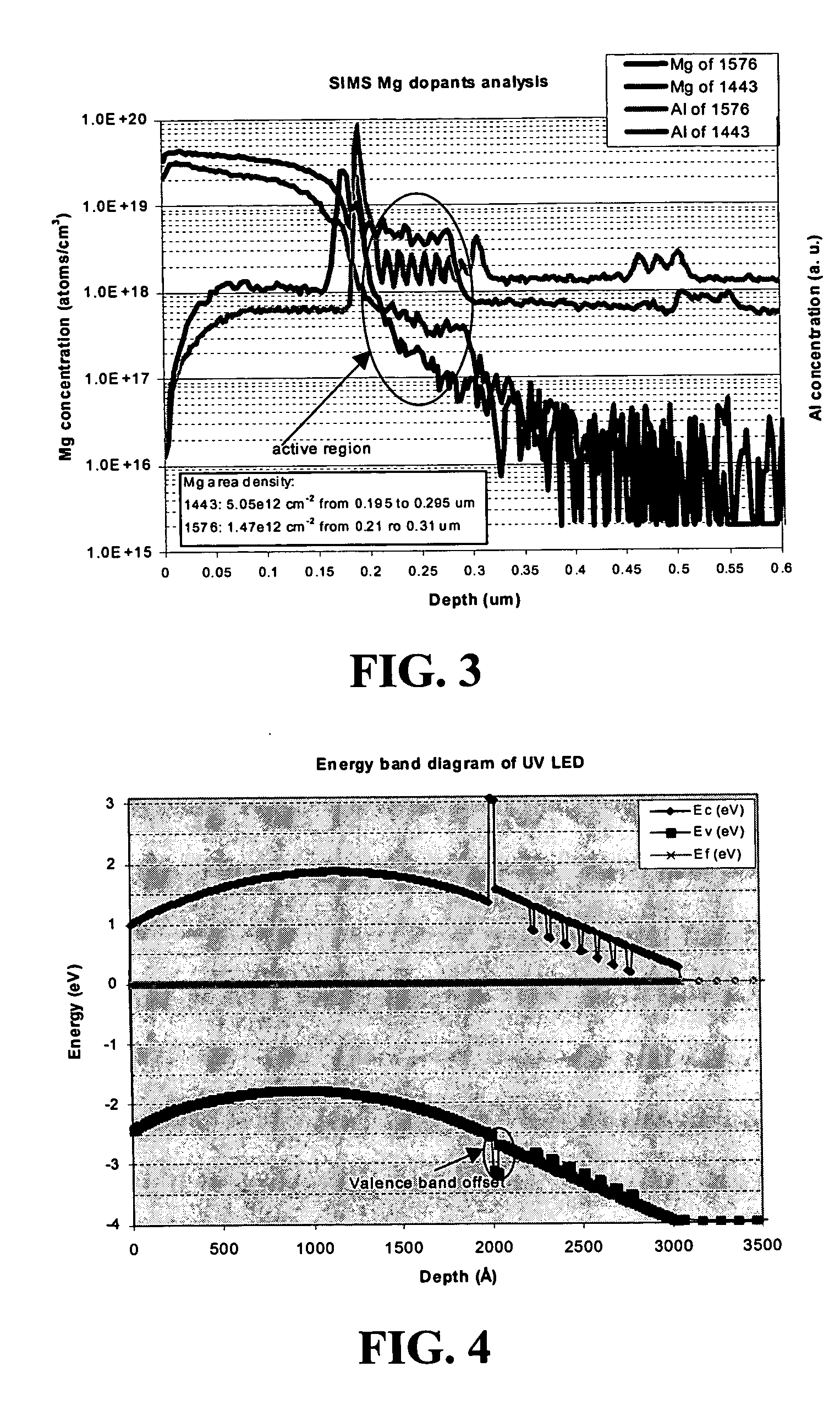
[0072] The high-Al AlGaN barrier layer technology of the invention is usefully employed to fabricate III-nitride electronic device structures in which migration and / or diffusion of unwanted material, e.g., dopant species, into active regions of the III-nitride device structure is substantially reduced or even eliminated b...


PUM

PropertyMeasurementUnit
thicknessaaaaaaaaaa
thicknessaaaaaaaaaa
thicknessaaaaaaaaaa

Abstract

A III-nitride electronic device structure including doped material, an active region and a barrier material arranged to suppress transport of dopant from the doped material into the active region, wherein the barrier material comprises high-Al content AlxGayN, wherein x+y=1, and x>=0.50. In a specific aspect, AIN is used as a migration/diffusion barrier layer at a thickness of from about 5 to about 200 Angstroms, to suppress flux of magnesium and/or silicon dopant material into the active region of the III-nitride electronic device, e.g., a UV LED optoelectronic device.

Description

[0001] 1. Field of the Invention[0002] This invention relates to III-nitride electronic and optoelectronic devices, and specifically to III-nitride electronic and optoelectronic device structures having a diffusion barrier of high-Al content Al.sub.xGa.sub.yN, wherein x+y=1, and x.gtoreq.0.50, and to methods of making same. The high-Al content Al.sub.xGa.sub.yN layer permits electronic and optoelectronic devices to be manufactured that are uncompromised by migration or diffusion of dopant species (e.g., magnesium, silicon, etc.) into the active device region, during the high temperature fabrication steps involving in the manufacture of such electronic and optoelectronic devices, including epitaxial growth and device fabrication.[0003] 2. Description of the Related Art[0004] In the manufacture of III-nitride optoelectronic devices, commonly employed dopants such as silicon and magnesium readily migrate or diffuse into active regions of the device structure during high temperature pro...

Claims


Application Information

Patent Timeline
Patent Type & Authority Applications(United States)
IPC IPC(8): H01L33/02H01L33/32
CPCH01L33/32H01L33/02
Inventor FLYNN, JEFFREY S.XIN, HUOPINGBRANDES, GEORGE R.
Owner CREELED INC
Why Eureka
Try Eureka