Multi-chip packages having a plurality of flip chips and methods of manufacturing the same

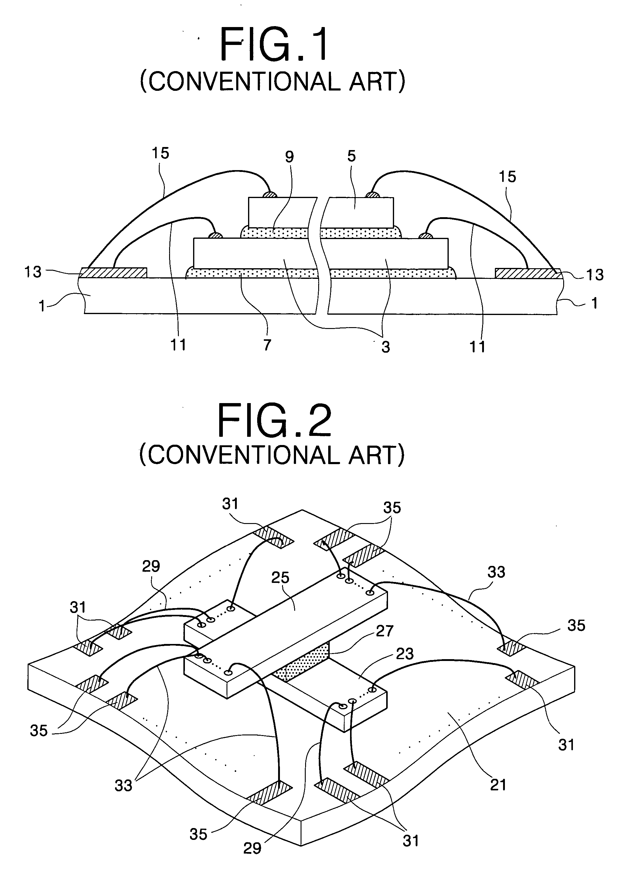
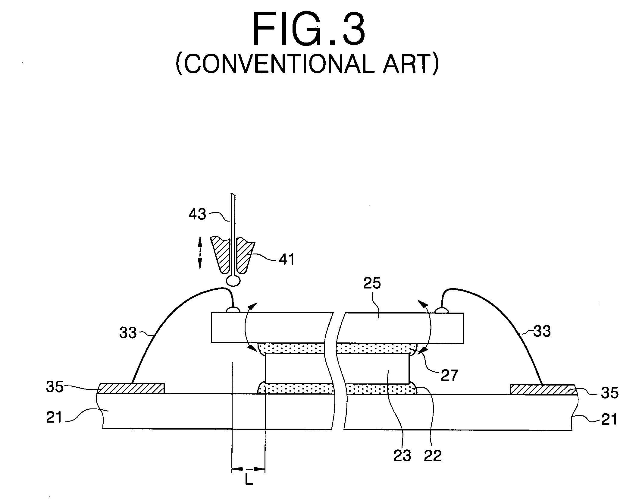
a technology of flip chips and multi-chip packages, which is applied in the field of multi-chip packages having a plurality of flip chips, can solve the problems of failure of contact of the second group of bonding wires 33

Inactive Publication Date: 2004-12-30
SAMSUNG ELECTRONICS CO LTD
View PDF15 Cites 154 Cited by
  • Summary
  • Abstract
  • Description
  • Claims
  • Application Information

AI Technical Summary

Problems solved by technology

Warpage of the overhangs may cause the contact of the second group of bonding wires 33 to fail.

Method used


Image

  • Multi-chip packages having a plurality of flip chips and methods of manufacturing the same
  • Multi-chip packages having a plurality of flip chips and methods of manufacturing the same
  • Multi-chip packages having a plurality of flip chips and methods of manufacturing the same

Examples


Embodiment Construction

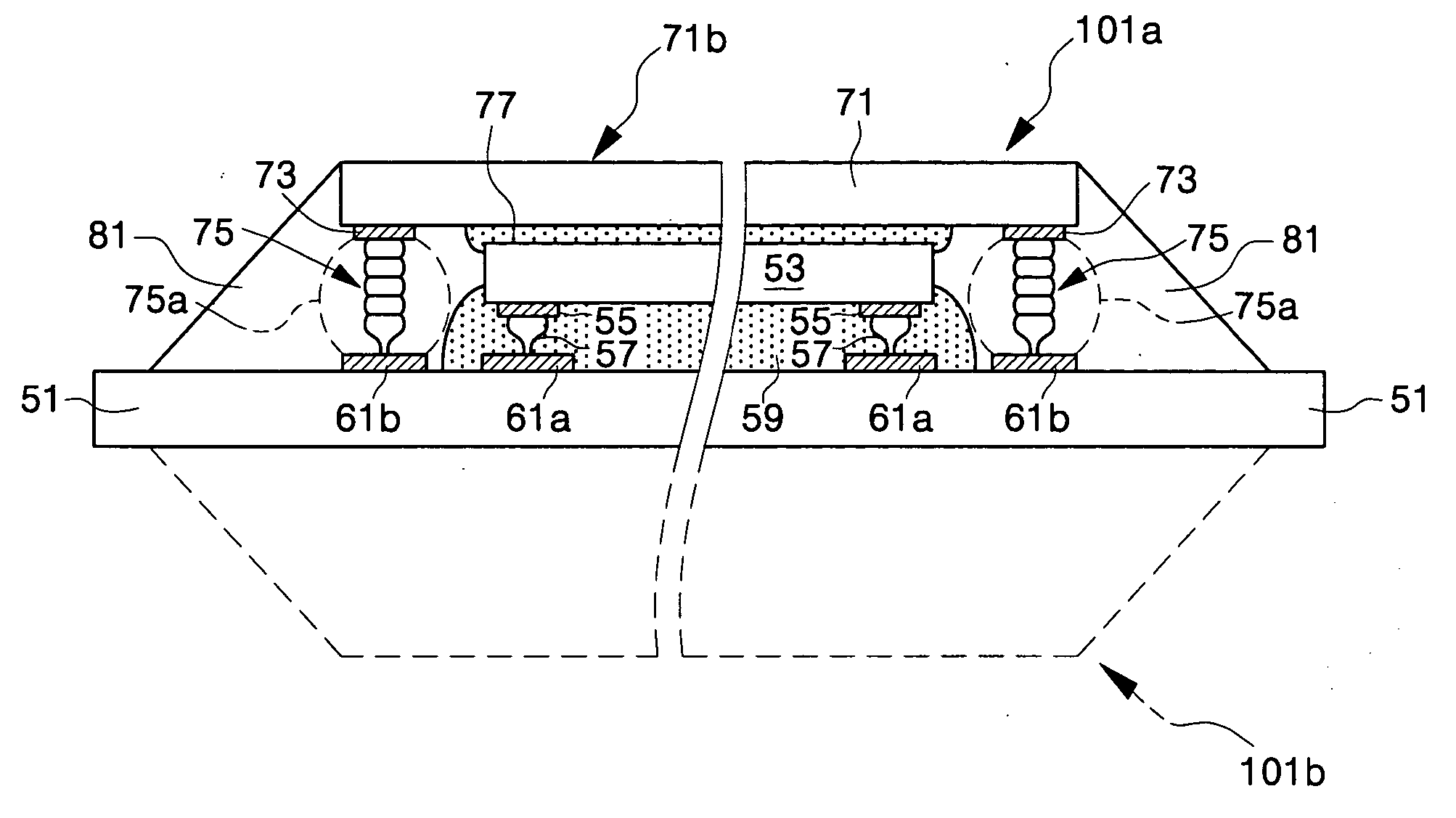
[0036] The present invention will now be described more fully hereinafter with reference to the accompanying drawings, in which exemplary embodiments of the invention are shown. However, the present invention may be embodied in different forms and should not be construed as limited to the exemplary embodiments set forth herein. Rather, these exemplary embodiments are provided for the purpose of illustration; the present invention covers various changes in form and details as will be readily contemplated by those ordinarily skilled in the art.

[0037] It should also be noted that the thickness of various layers and regions in the stacked package have been exaggerated in the drawings for the purpose of clarity and the same drawing reference numerals are used for the same elements even in different drawings.

[0038] It should also be noted that a layer is considered as being formed "on" another layer or substrate when formed either directly on the referenced layer or the substrate or forme...


PUM


Abstract

Multi-chip packages having at least two flip chips and methods of manufacturing the same are provided. The multi-chip packages may include a printed circuit board having a substrate and a plurality of interconnection lines formed on a front surface of the substrate. The at least two flip chips may be stacked on the front surface of the substrate. The flip chips may be stacked so that pads of the flip chips face the printed circuit board. A first group of bumps may be interposed between the pads of the first flip chip and a first group of interconnection lines of the plurality of lines. Further, a second group of bumps may be interposed between the pads of the at least one upper flip chip and a second group of interconnection lines of the plurality of lines.

Description

[0001] This application claims the benefit of priority of Korean Patent Application No. 2003-0042730, filed Jun. 27, 2003, the contents of which are herein incorporated by reference in their entirety.[0002] 1. Field of the Invention[0003] The present invention relates to semiconductor packages and, more particularly, to multi-chip packages having a plurality of flip chips and methods of manufacturing the same.[0004] 2. Description of the Related Art[0005] As portable electronic devices become smaller, semiconductor packages mounted in the portable electronic devices have been also become smaller. Further, a technique for mounting a plurality of semiconductor chips in a single semiconductor package, e.g., a multi-chip package technique has been used in order to increase the capacity of the package.[0006] FIG. 1 is a sectional view illustrating a conventional multi-chip package. Referring to FIG. 1, a lower chip 3 and an upper chip 5 may be stacked on a printed circuit board 1. A back...

Claims


Application Information

Patent Timeline
Patent Type & Authority Applications(United States)
IPC IPC(8): H01L21/56H01L23/12H01L25/18H01L23/485H01L23/495H01L25/065H01L25/07
CPCH01L21/563H01L23/49575H01L24/45H01L25/0657H01L2224/1134H01L2224/1308H01L2224/131H01L2224/13144H01L2224/32145H01L2224/45144H01L2224/48091H01L2224/48465H01L2224/73203H01L2224/73265H01L2225/06562H01L2924/01004H01L2924/01015H01L2924/01029H01L2924/01033H01L2924/01079H01L2924/01082H01L2924/14H01L2924/19042H01L2924/19043H01L2924/30105H01L2924/30107H01L24/48H01L2924/00013H01L2924/01005H01L2924/01006H01L2924/01068H01L2924/01087H01L2924/014H01L2224/16225H01L2224/32225H01L2224/73204H01L2224/73253H01L2224/45147H01L2924/01028H01L24/78H01L2224/78301H01L24/11H01L24/13H01L2924/00014H01L2224/13099H01L2924/00H01L2224/48227H01L2924/00012H01L2924/181H01L24/73H01L2924/18161H01L2224/11H01L2224/13H01L2224/05573H01L2224/05568H01L2224/05599H01L23/12
Inventor KANG, IN-KUKIM, JIN-HOAN, SANG-HO
Owner SAMSUNG ELECTRONICS CO LTD
Why Eureka
Try Eureka