Digital bus monitor integrated circuits

a digital bus and integrated circuit technology, applied in the field of electronic circuits, can solve the problems of ineffective speed detection at speed functional problems, inability to dynamically detect at speed, and expensive test equipment required to dynamically monitor

Inactive Publication Date: 2005-01-06
TEXAS INSTR INC
View PDF99 Cites 1 Cited by
  • Summary
  • Abstract
  • Description
  • Claims
  • Application Information

AI Technical Summary

Benefits of technology

[0006] In accordance with the present invention, a digital bus monitor is provided which substantially eliminates or prevents the disadvantages and problems associated with prior digital bus testing devices.
[0008] The digital bus monitor of the present invention provides several technical advantages over the prior art. The digital bus monitors of the present invention may be imbedded in the board design and can be activated throughout the life cycle of the board, from production testing to field service and maintenance. Another advantage is that the digital bus monitors do not impede the performance of the board's circuitry. Since the input signals to be monitored do not have to be routed through the digital bus monitor, but are only input to the digital bus monitor, no significant functional performance penalty is paid while using these devices.
[0010] The digital bus monitor of the present invention provides the advantage of analyzing data on data buses coupling multiple integrated circuits while the integrated circuits are operating at speed. The at speed testing of the integrated circuits detect errors that might not otherwise be found.

Problems solved by technology

Traditionally, expensive test equipment has been required to dynamically monitor the functional interactions of integrated circuits on a board design.
Other techniques such as boundary scan provide off-line or static testing of wiring interconnects between integrated circuits, but are not effective in detecting at speed functional problems that can occur in the bussing paths between integrated circuits.
Such a test can reveal timing sensitive and / or intermittent failures that would otherwise not be detectable without the use of expensive testers and mechanical probing fixtures.
Heretofore, the ability to dynamically observe digital buses between integrated circuits has been unavailable.
Current test methods used to monitor or observe signal paths between integrated circuits on board designs require the use of expensive external tester equipment and signal node probing mechanisms.
One problem with the current test approach is that state-of-the-art board designs are so densely populated with integrated circuits that physical probing of the signal paths is very difficult, if not impossible.
Another problem is that the board tester is dependent upon the availability of external testers and probing fixtures.
Transportation and upkeep of the required test equipment in a field environment to support a system can be a very expensive proposition.

Method used


Image

  • Digital bus monitor integrated circuits
  • Digital bus monitor integrated circuits
  • Digital bus monitor integrated circuits

Examples


Embodiment Construction

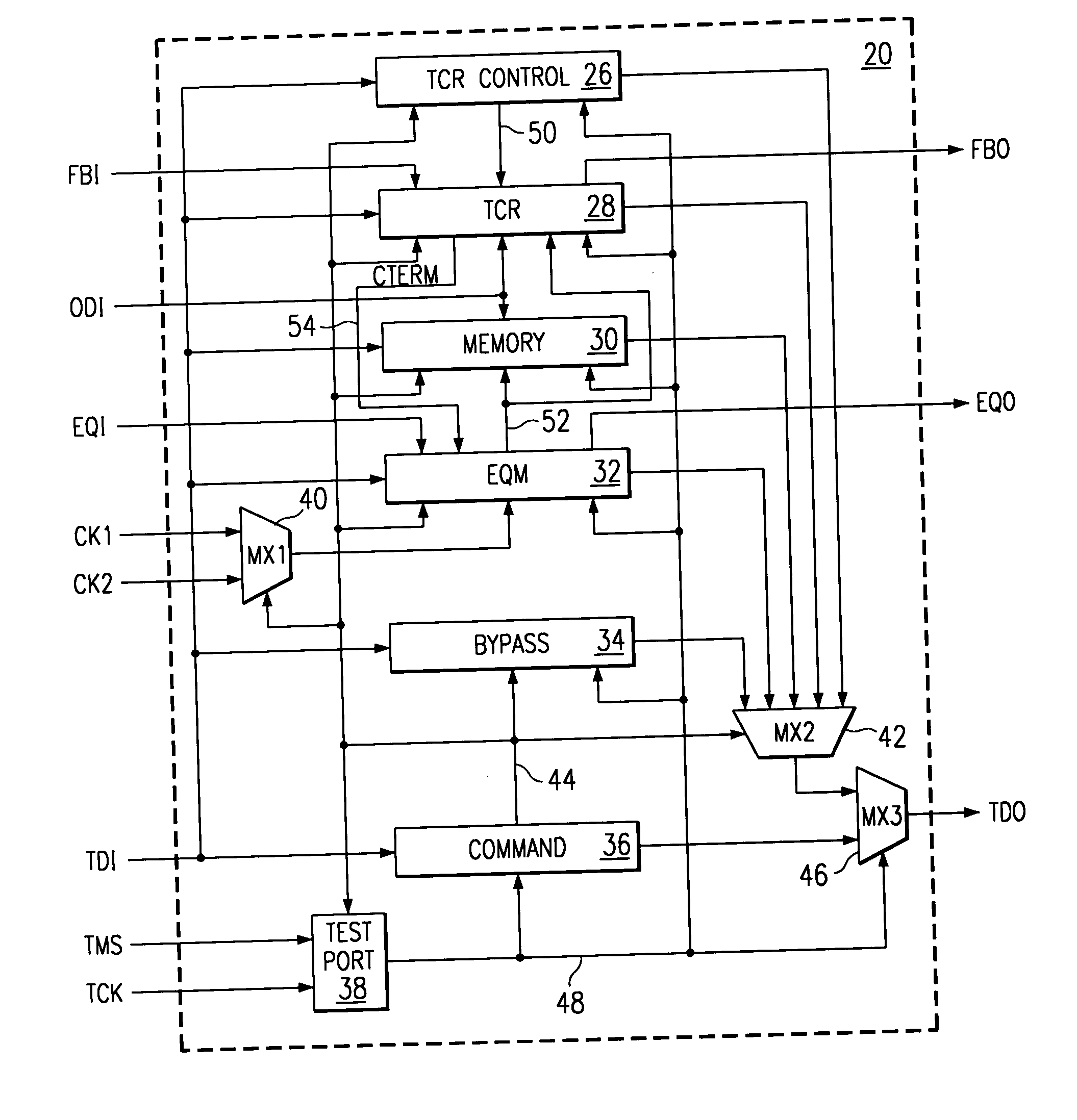
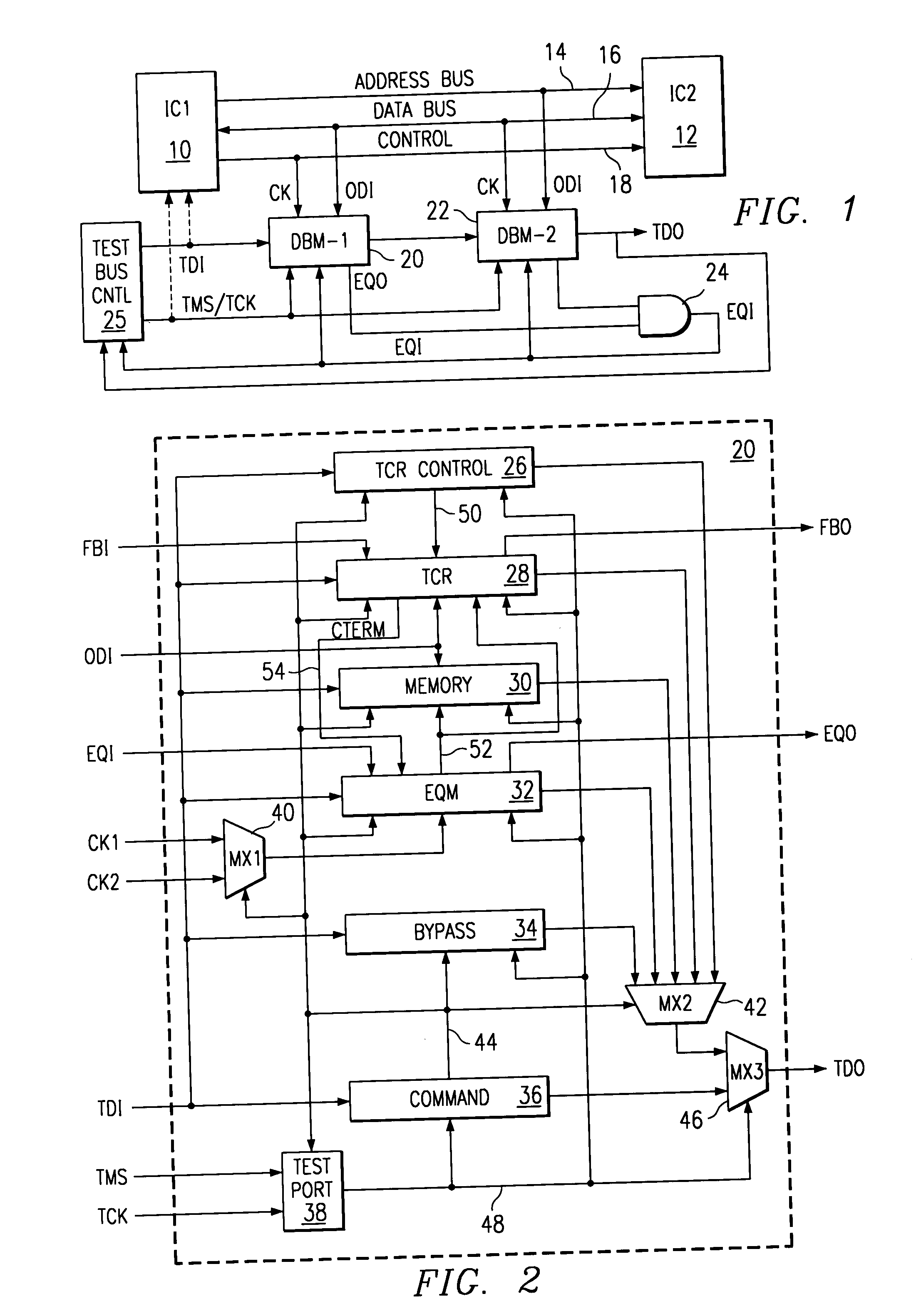
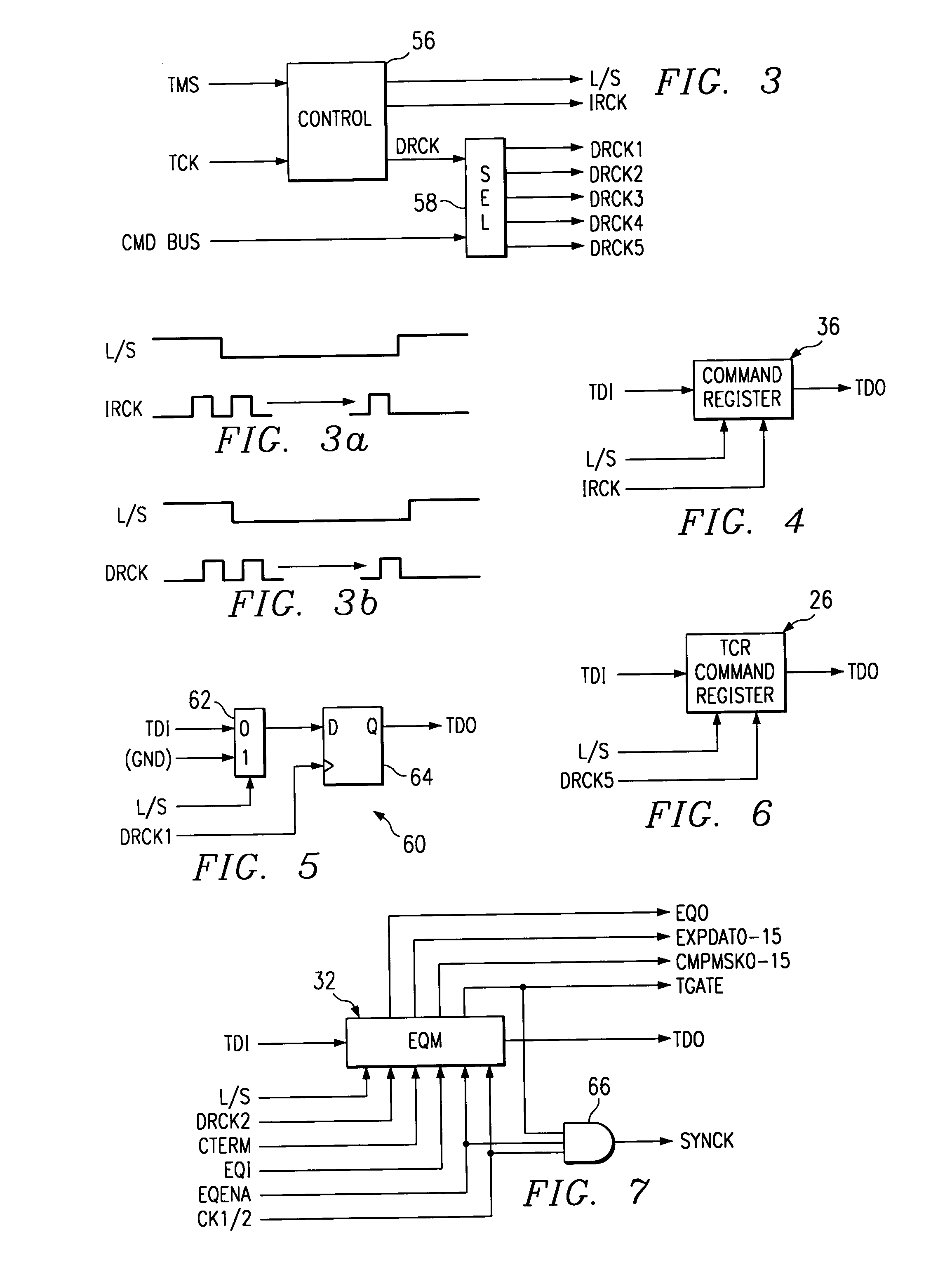
[0032] The preferred embodiment of the present invention is best understood by referring to FIGS. 1-10 of the drawings, like numerals being used for like and corresponding parts of the various drawings.

[0033] Digital Bus Monitor Application

[0034]FIG. 1 illustrates a block diagram of an exemplary circuit using the digital bus monitor (DBM) of the present invention. As illustrated in FIG. 1, two integrated circuits, IC110 and IC212, are connected by three buses: An address bus 14, a data bus 16, and a control bus 18. A first data bus monitor DBM120 is connected to the control bus 18 by its CK and input to the data bus 16 via its ODI (observability data input) input. The second data bus monitor DBM222 is connected to the control bus 18 via its CK input and to the address bus 14 via its ODI input. DBM120 and DBM222 are interconnected together via a serial scan path connection comprising a test data input (TDI) and a test data output (TDO). The TDO of DBM120 is connected to the TDI of ...


PUM


Abstract

A digital bus monitor used to observe data on a bus (14, 16, 18) connecting multiple integrated circuits (10, 12) comprises a memory buffer (30), bypass register (34), test port (38) and output control circuits (42, 46) controlled by an event qualifying module (EOM) (32). In response to a matching condition the EQM (32) may perform a variety of tests on incoming data while the integrated circuits (10, 12) continue to operate at speed. A plurality of digital bus monitors (20, 22) may be cascaded for observation and test of variable width data buses and variable width signature analysis.

Description

TECHNICAL FIELD OF THE INVENTION [0001] This invention relates in general to electronic circuits, and more particularly to a digital bus monitor for observing and controlling data on a bus connecting multiple integrated circuits. BACKGROUND OF THE INVENTION [0002] Traditionally, expensive test equipment has been required to dynamically monitor the functional interactions of integrated circuits on a board design. During test, the integrated circuits are made to operate together functionally while an external tester observes the transactions occurring between the integrated circuits. Other techniques such as boundary scan provide off-line or static testing of wiring interconnects between integrated circuits, but are not effective in detecting at speed functional problems that can occur in the bussing paths between integrated circuits. [0003] The ability to dynamically (i.e., during normal operation of the circuit board) observe the data passing between integrated circuits in real-time...

Claims


Application Information

Patent Timeline
Patent Type & Authority Applications(United States)
IPC IPC(8): G06F11/22G01R31/28G01R31/3185G06F11/00G06F11/267G06F11/30G06F13/00G06F13/38
CPCG01R31/31855G01R31/318555G06F11/221G01R31/318572G01R31/318569
Inventor WHETSEL, LEE DOYLE
Owner TEXAS INSTR INC
Why Eureka
Try Eureka