
Nonvolatile memory unit with specific cache

a memory unit and cache technology, applied in the field of digital data storage systems, can solve the problems of high power consumption, inability to withstand physical shock, high power consumption, etc., and achieve the effect of reducing the frequency of swap operation

Inactive Publication Date: 2005-01-20
SOLID STATE SYST
View PDF5 Cites 396 Cited by
  • Summary
  • Abstract
  • Description
  • Claims
  • Application Information

AI Technical Summary

Benefits of technology

[0015] One of the objectives in the present invention is to reduce the frequency of swap operation when a random write occurs by introducing a specific cache area and a directory cache area, when the data belonging to the two specific types are to be written.
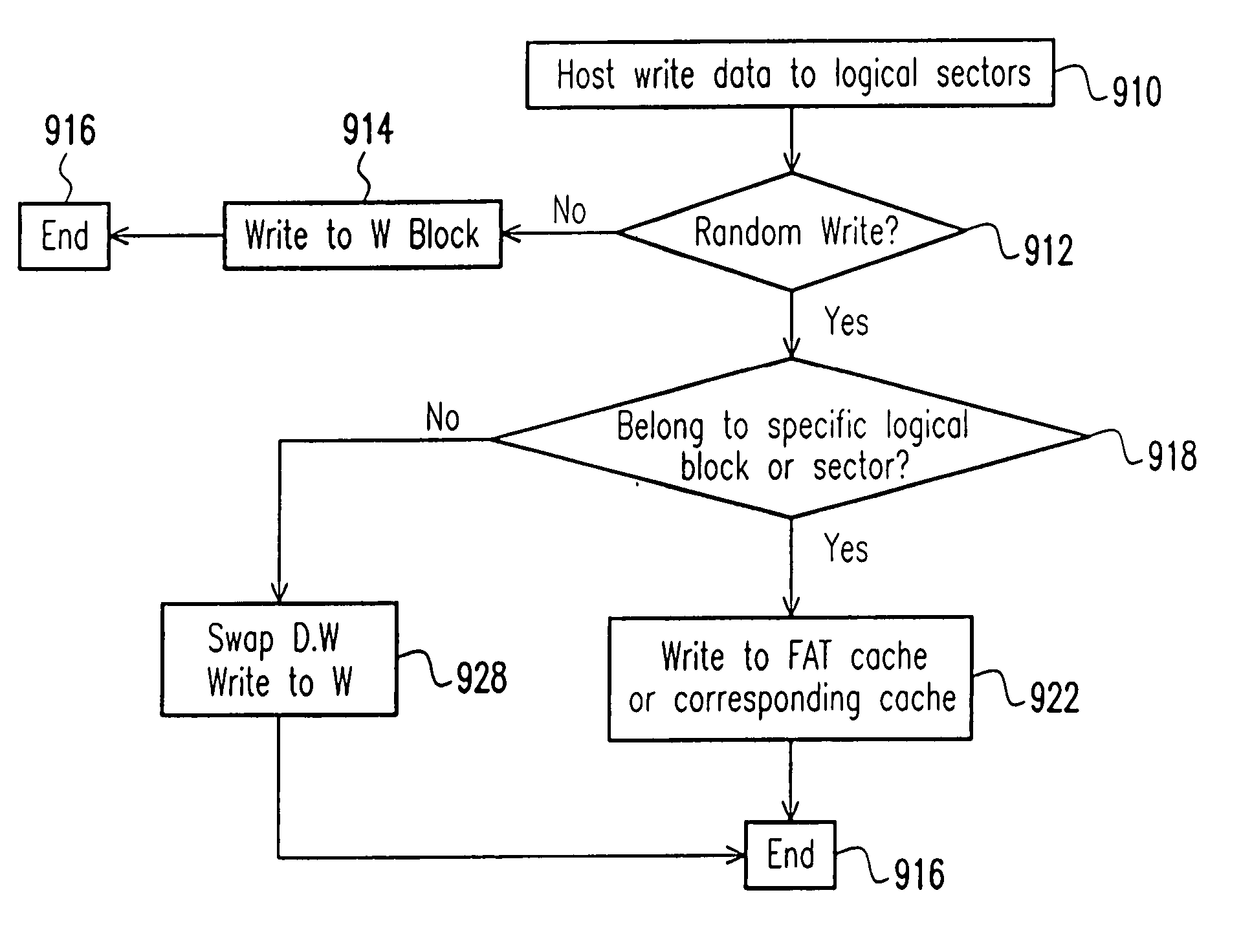
[0016] The invention provides a method for organizing a writing operation to a nonvolatile memory. The method comprises setting a specific cache area, into which a specific data belonging to a specific group of logical blocks is to be written. It is determined whether or not the writing operation is a random write. If the writing operation is the random write, then the following steps are performed: determining whether or not the writing operation is to write a data that is belonging to the specific group of logical blocks; and writing the data into the specific cache area if the data is belonging to the specific group of logical blocks. As a result, a swap action between a data block and a writing block can be avoided during a random write operation.
[0017] The invention provides another method for organizing a writing operation to a nonvolatile memory. The method comprises setting a specific cache area. It is determined whether or not the writing operation is a random write. If the writing operation is the random write, then the following steps are performed: determining whether or not a sector count of a data to be written is less than a predetermined number; and writing the data into the specific cache area if the sector count of the data is less than the predetermined number. Wherein, a swap action between a data block and a writing block can be avoided during a random write operation.
[0018] The invention further provides a method for organizing a writing operation to a nonvolatile memory. The method comprises setting a specific cache area. It is determined whether or not the writing operation is a random write. If the writing operation is the random write, then the following steps are performed. It is determined whether or not the writing operation is to write a data that is belonging to the specific group of logical blocks. The data is written into the specific cache area if the data is belonging to the specific group of logical blocks. It is determined whether or not a sector count of the data to be written is less than a predetermined number. The data is written into the specific cache area if the sector count of the data is less than the predetermined number. Wherein, a swap action between a data block and a writing block can be avoided during a random write operation.

Problems solved by technology

Although hard disk drives are widely used in current computer system, the hard disk still has several deficiencies such as rotation and high power consumption, in which consumption magnetic mass storage devices, like an inherent latency during accessing the hard disk drives, high power consumption, being unable to withstand the physical shock, and having a large weight for portable computer devices.
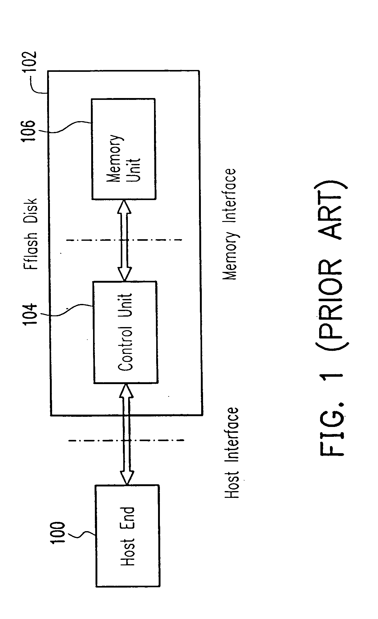
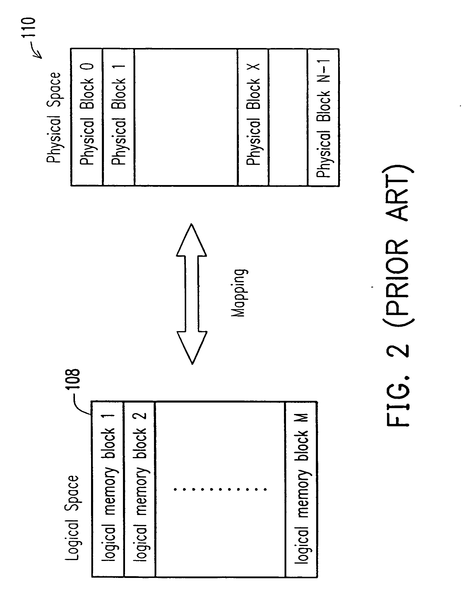
Indeed, the host can not directly address the physical space so that the controller must maintain the mapping relations between the logical blocks and the physical blocks.
However, since the overhead arises from erase-then-program architecture, when the data will be re-written into the data block 302, the data is temporarily written to a writing block 304.
The swap operation we have to do now is time-consuming and reduces the system performance.
Since the swap action between the data block and the writing block consumes more cycle time, this would seriously reduced the writing speed.

Method used


Image

  • Nonvolatile memory unit with specific cache
  • Nonvolatile memory unit with specific cache
  • Nonvolatile memory unit with specific cache

Examples


Embodiment Construction

[0038] One of the features of the present invention is to reduce the frequency of swap action when a random write is required to the nonvolatile memory unit within the memory storage device. After inspecting the types of random write, the present invention found that the random write resulting in a swap action will always occur when the host writes FAT or directory information into the memory storage device during file access. The present invention then propose to create a specific cache area, which can include, for example, the FAT cache for storing the FAT-like information, the directory cache for storing the directory-like information, or other corresponding cache for storing data belonging to a specific logical sector or logical block. Each FAT or directory cache is comprised of at least one physical block. As a result, some kinds of random write will not be necessary to take the swap action in each time of data write. Then, the data writing speed can be effectively improved. An...


PUM


Abstract

The invention provides a method for organizing a writing operation to a nonvolatile memory. The method comprises setting a specific cache area, into which a specific data belonging to a specific group of logical blocks is to be written. It is determined whether or not the writing operation is a random write. If the writing operation is the random write, then the following steps are performed: determining whether or not the writing operation is to write a data that is belonging to the specific group of logical blocks; and writing the data into the specific cache area if the data is belonging to the specific group of logical blocks. As a result, a swap action between a data block and a writing block can be avoided during a random write operation. A storage structure in a nonvolatile memory device are organized to perform the forgoing writing operation.

Description

BACKGROUND OF THE INVENTION [0001] 1. Field of Invention [0002] The present invention relates to digital data storage systems using a non-volatile memory device. More particularly, the present invention relates to the non-volatile memory unit including a specific cache, such as a FAT cache, so as to reduce the frequency for swapping action during writing data into the non-volatile memory unit. [0003] 2. Description of Related Art [0004] Although hard disk drives are widely used in current computer system, the hard disk still has several deficiencies such as rotation and high power consumption, in which consumption magnetic mass storage devices, like an inherent latency during accessing the hard disk drives, high power consumption, being unable to withstand the physical shock, and having a large weight for portable computer devices. A non-volatile memory mass storage device, like a flash memory disk drive, is a nice choice for replacing a hard disk. Each memory mass storage device al...

Claims


Application Information

Patent Timeline
Patent Type & Authority Applications(United States)
IPC IPC(8): G06F3/06G06F12/02G06F12/08G06F12/0875G11C
CPCG06F3/0613G06F3/064G06F3/0679G06F2212/7207G06F12/0875G06F2212/7203G06F12/0246
Inventor WANG, CHIH-HUNGKUO, CHUN-HAOLIN, CHUN-HUNG
Owner SOLID STATE SYST
Learn More