

System and method for providing a redundant memory array in a semiconductor memory integrated circuit
a technology of memory array and integrated circuit, which is applied in the direction of information storage, static storage, digital storage, etc., can solve the problem of increasing the probability of a defective circuit element on the integrated circuit, and achieve the effect of improving the probability of a defective circuit elemen
- Summary
- Abstract
- Description
- Claims
- Application Information
AI Technical Summary
Benefits of technology
Problems solved by technology
Method used
Image

Examples
Embodiment Construction
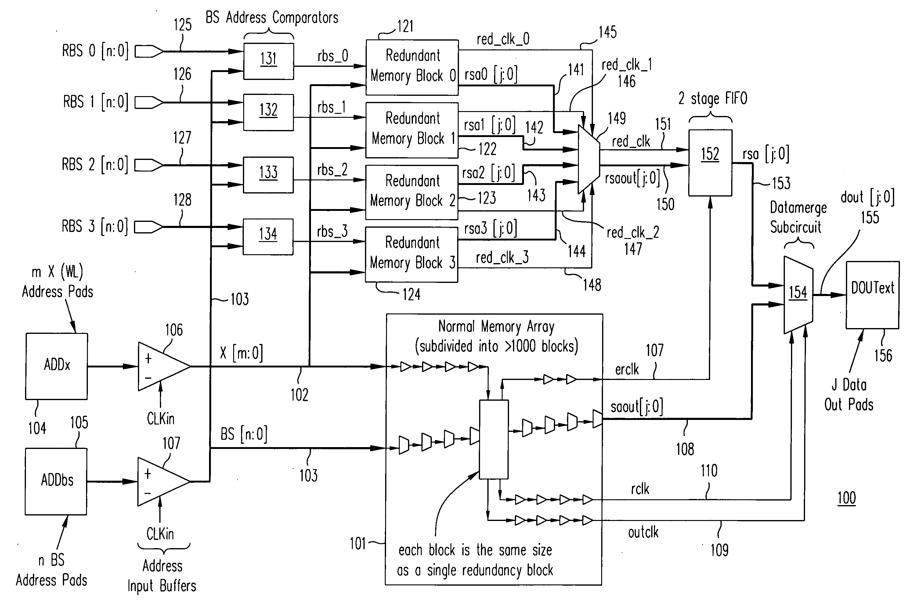
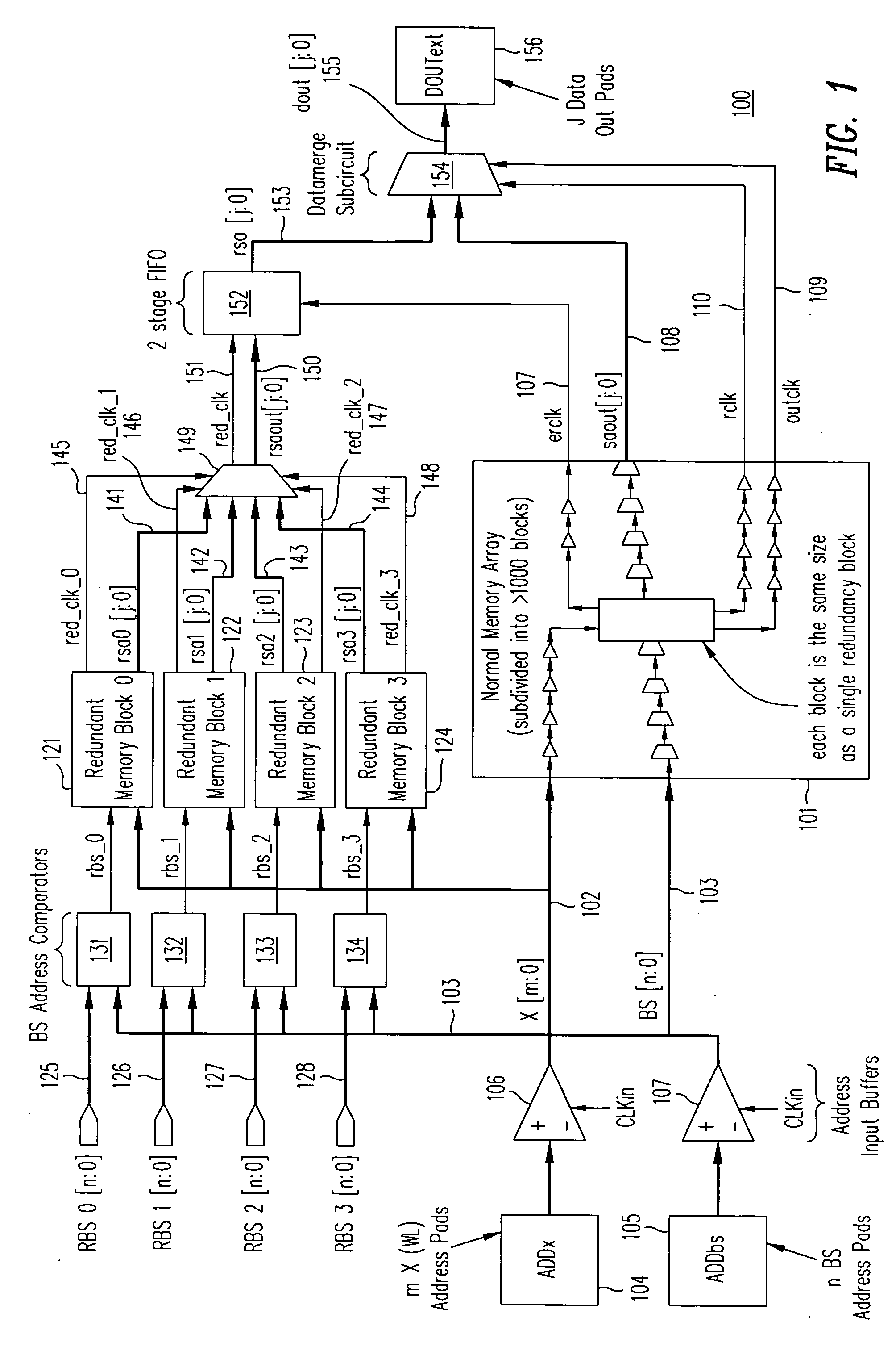
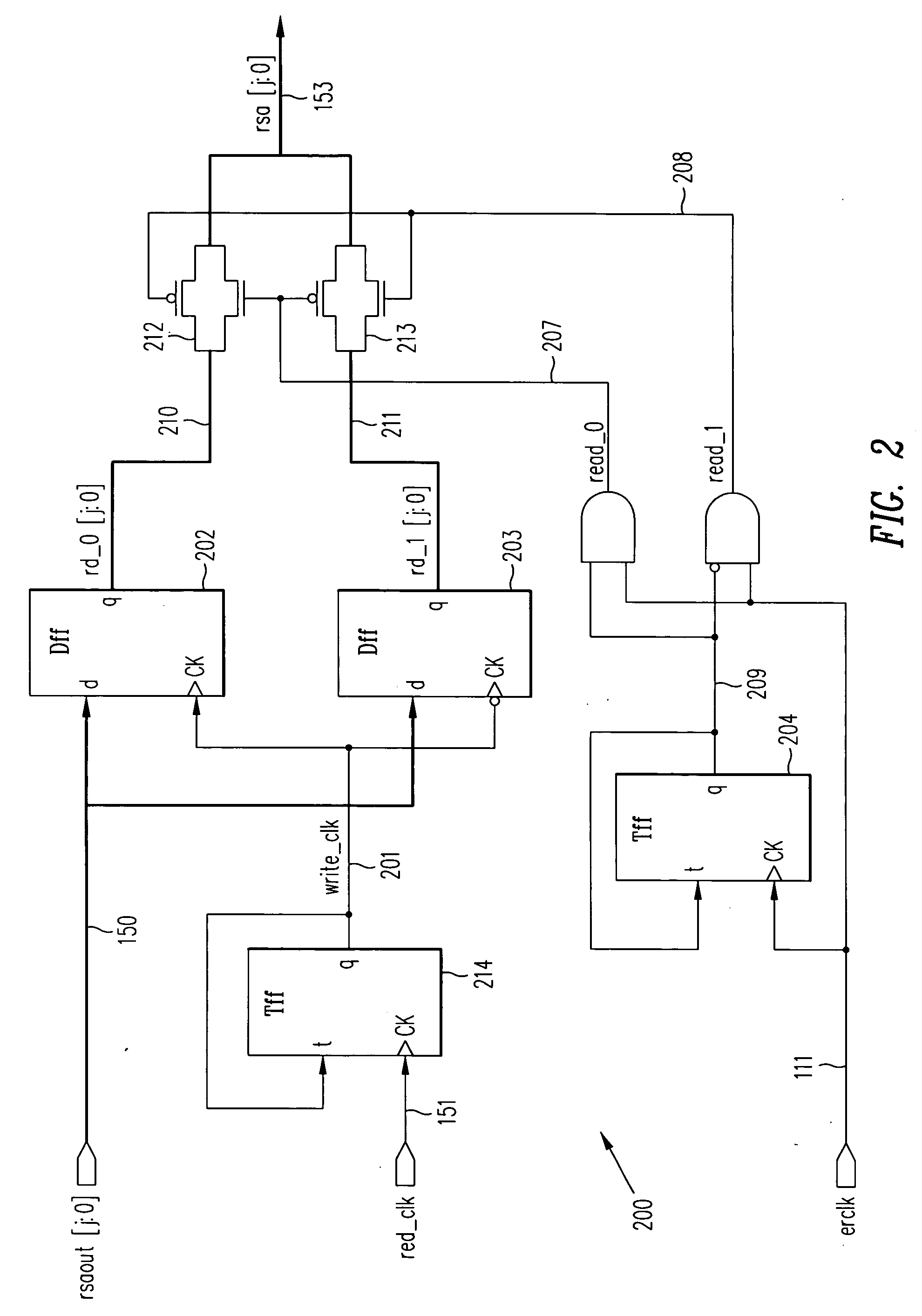
[0021] The present invention provides a memory device with redundant memory blocks that can be configured to substitute for defective blocks in the main memory array with correct timing and correct order of data output. FIG. 1 shows memory circuit 100, according to one embodiment of the present invention.
[0022] As shown in FIG. 1, memory circuit 100 includes main memory array 101 and redundant blocks 121-124. Main memory array 101 includes an array of numerous conventional memory blocks (e.g., 1024), each of which includes conventional column and row decoders, and conventional sense amplifiers and output circuits. (Of course, the number of memory blocks in main memory array 101 and the number of redundant blocks shown herein are merely illustrative; the present invention is applicable to any number of memory blocks in the main memory array and any number of redundant memory blocks.) Main memory array 101, which is pipelined to enhance throughput, receives an (m+1)-bit “X” address X...
PUM
 Abstract
Description
Claims
Application Information