Placement and optimization of process dummy cells

a technology of dummy cells and process, applied in the direction of computer aided design, total factory control, instruments, etc., can solve the problems of affecting the efficiency of dummy cells, affecting the yield of dummy cells, and unable to achieve anything inside cells

Active Publication Date: 2012-07-17
GLOBALFOUNDRIES U S INC
View PDF21 Cites 105 Cited by
  • Summary
  • Abstract
  • Description
  • Claims
  • Application Information

AI Technical Summary

Benefits of technology

[0017]Dummy cells may be used to improve process latitude, but they can contribute to yield loss if they are shorted to active circuitry / cells, or to other features of the memory array such at word lines or bitlines. For example, a short between a bitline contact to poly (word line) may drag down the voltage on bitline and cause the whole bitline to fail. A defect of an inside cell will, of course, cause the same problem, but there is generally nothing that can be done to the inside cells since they are used for circuit functions. But the dummy cells can be modified to significantly reduce the probability of such failures.
[0019]Optimize dummy cells to reduce failures in dummy cells or between dummy cells and inside cells

Problems solved by technology

Dummy cells may be used to improve process latitude, but they can contribute to yield loss if they are shorted to active circuitry / cells, or to other features of the memory array such at word lines or bitlines.
For example, a short between a bitline contact to poly (word line) may drag down the voltage on bitline and cause the whole bitline to fail.
A defect of an inside cell will, of course, cause the same problem, but there is generally nothing that can be done to the inside cells since they are used for circuit functions.

Method used


Image

  • Placement and optimization of process dummy cells
  • Placement and optimization of process dummy cells
  • Placement and optimization of process dummy cells

Examples


embodiment 1

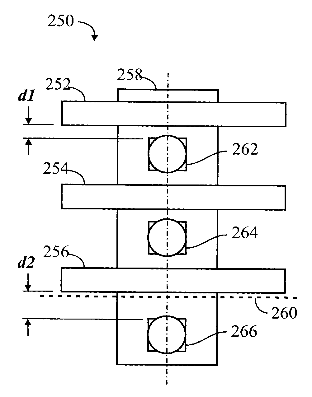
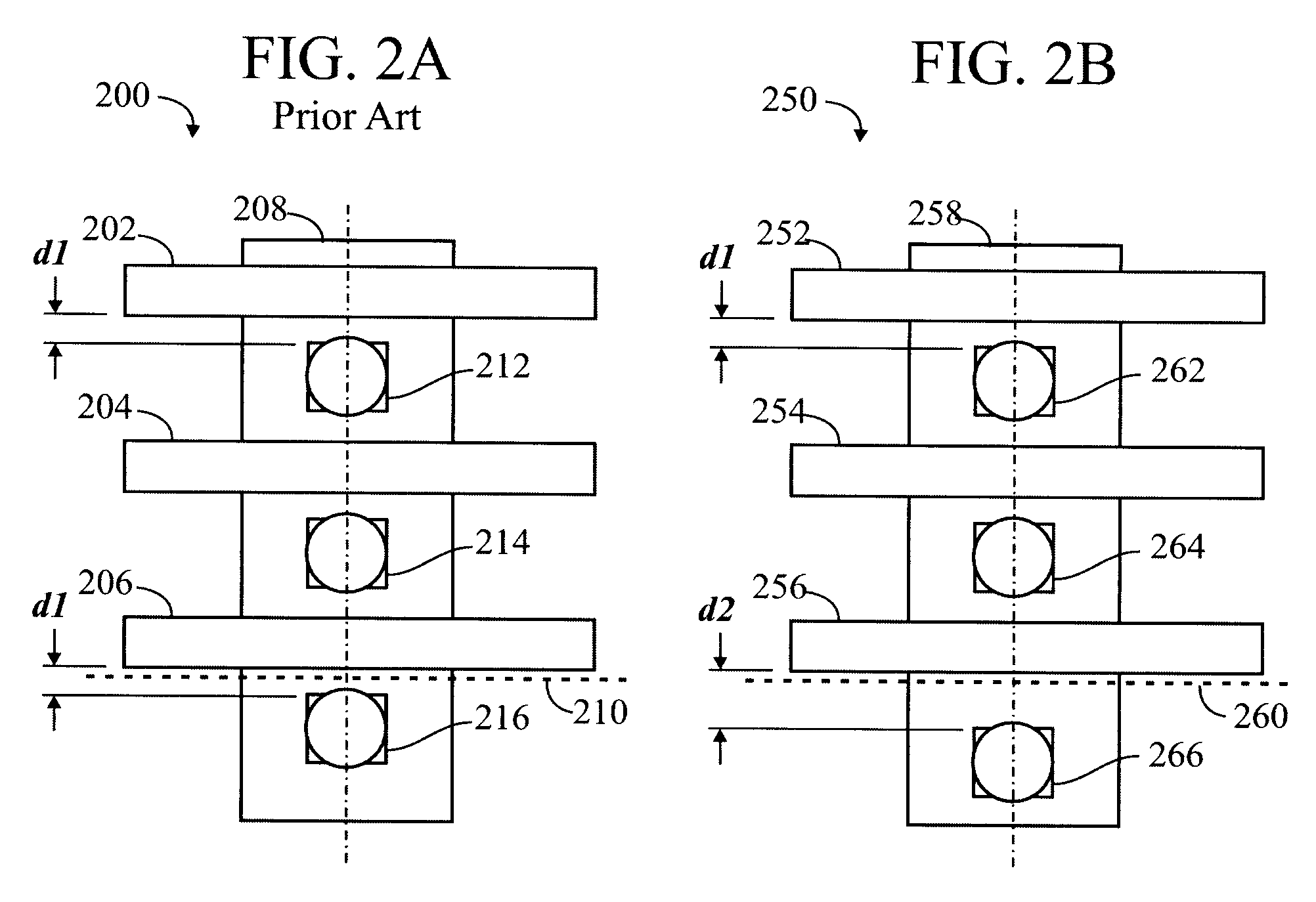
[0053]An embodiment of the invention is illustrated with respect to FIGS. 2A and 2B.

[0054]FIG. 2A illustrates a portion of an exemplary memory array 200, according to the prior art. Various layers of materials are illustrated.

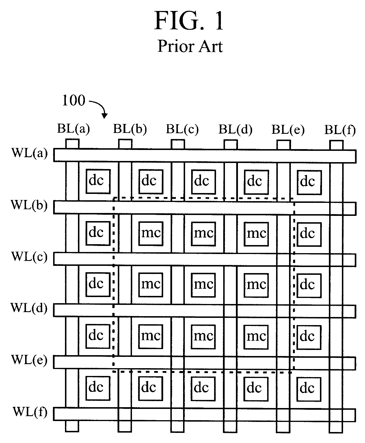
[0055]Three polysilicon lines 202, 204, 206 are shown traversing an active area 208. The polysilicon lines may be wordlines, and may be evenly spaced from one another. (The “active area”208 describes an area of silicon where devices may be fabricated, and should not be confused with active array area, such as within the rectangular box in FIG. 1.)

[0056]A dashed line 210 represents an edge of a cell area of the array. Above the line 210 are active memory cells “mc” (see FIG. 1). Below the line 210 are dummy dells “dc” or process dummy patterns (see FIG. 1).

[0057]Three structures 212, 214 and 216, are shown, each of which is placed a distance d1 below a corresponding one of the poly lines 202, 204 and 206. The structures 212, 214 and 216 may be contacts, or bitli...

embodiment 2

[0093]A second embodiment of the invention is illustrated with respect to FIGS. 4A and 4B.

[0094]Some users may not have resources and available yield models to perform all of the calculations in the previous embodiment (Approach 1). The embodiment described hereinbelow (Approach 2) is at lithography / etch simulation level only, and is computationally simpler. The software customers may be different: Approach 1 is for the yield community, and Approach 2 is for the lithography community. Lithographers spend a lot of time maximizing “process windows” and this is geared toward this purpose. Assuming no yield loss in the dummy itself, maximizing process window will typically increase yield as well.

[0095]FIG. 4A is essentially the same as FIG. 2A, and illustrates a portion of an exemplary memory array 200, according to the prior art. Various layers of materials are illustrated.

[0096]Three polysilicon lines 402, 404, 406 are shown traversing an active area 408. The polysilicon lines may be ...


PUM


Abstract

A method for laying out process dummy cells in relationship to inside memory cells of a memory array includes (a) calculating an initial process performance parameter for the memory array; (b) changing dummy cell layout configuration for a layer electrically connected to inside cells; (c) applying lithographic simulation and yield model for both the inside memory cells and the changed layout configuration process dummy cells; and (d) repeating steps (b) and (c) until yield is maximized. Checks may be performed to ensure that there is enough room to make the change and that there is no significant adverse effect to neighboring circuits. The process performance parameter may be yield or a process window for the inside memory cells.

Description

FIELD OF THE INVENTION[0001]The invention relates to semiconductor device fabrication and, more particularly, to the use of dummy structures such as dummy cells which are process dummies.BACKGROUND OF THE INVENTION[0002]Integrated circuits (ICs) may incorporate many elements, structures and features, such as patterns of polysilicon, contacts and metal layers. A memory array, for example, may include a number of transistors, word lines, bitlines and contacts.[0003]The processes used for making ICs, such as lithography (sometimes referred to as printing) and etching (including chemical mechanical etching) may be sensitive to the uniform distribution and proximity of patterns of the elements, structures and features. Hence, it is generally known that certain benefits can be derived from incorporating “dummy” features into a design for an IC. These dummy features may be referred to as “process dummies”, since they do not perform any electrical function in the circuit. As used herein, a ...

Claims


Application Information

Patent Timeline
Patent Type & Authority Patents(United States)
IPC IPC(8): G06F17/50
CPCG11C5/02G11C29/24H01L27/0203H01L27/105G06F2217/12G06F2119/18Y02P90/02
Inventor OUYANG, XUHAN, GENGLIEBMANN, LARS W.
Owner GLOBALFOUNDRIES U S INC
Why Eureka
Try Eureka