Transistor, integrated circuit, electro-optic device, electronic instrument and method of manufacturing a transistor

a technology of integrated circuits and transistors, applied in the field of transistors, integrated circuits, electrooptic devices, electronic instruments and methods of manufacturing transistors, can solve the problems of current leakage, restriction, and other degradation, and achieve the effect of reducing material was

Inactive Publication Date: 2005-02-10
SEIKO EPSON CORP
View PDF8 Cites 37 Cited by
  • Summary
  • Abstract
  • Description
  • Claims
  • Application Information

AI Technical Summary

Benefits of technology

[0029] With this method there is little wastage of material and a predetermi

Problems solved by technology

These bumps and indentations can be a restriction when optimizing the wiring structure.
The differen

Method used


Image

  • Transistor, integrated circuit, electro-optic device, electronic instrument and method of manufacturing a transistor
  • Transistor, integrated circuit, electro-optic device, electronic instrument and method of manufacturing a transistor
  • Transistor, integrated circuit, electro-optic device, electronic instrument and method of manufacturing a transistor

Examples


Embodiment Construction

[0041] While preferred embodiments of the invention have been described and illustrated above, it should be understood that these are exemplary of the invention and are not to be considered as limiting. Additions, omissions, substitutions, and other modifications can be made without departing from the spirit or scope of the present invention. Accordingly, the invention is not to be considered as limited by the foregoing description and is only limited by the scope of the appended claims.

[0042] A description will now be given of the embodiments of the present invention with reference made to the drawings.

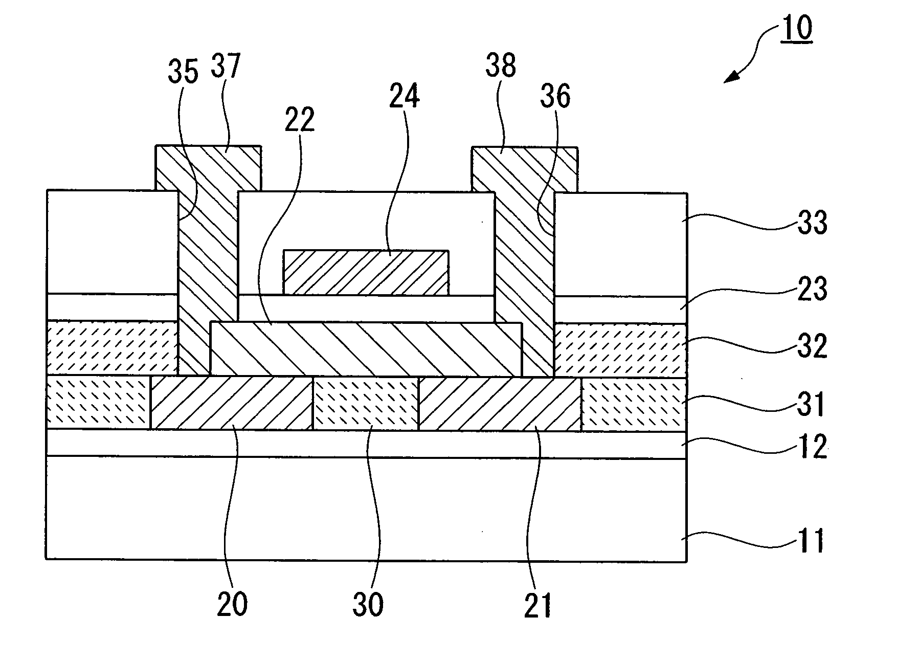
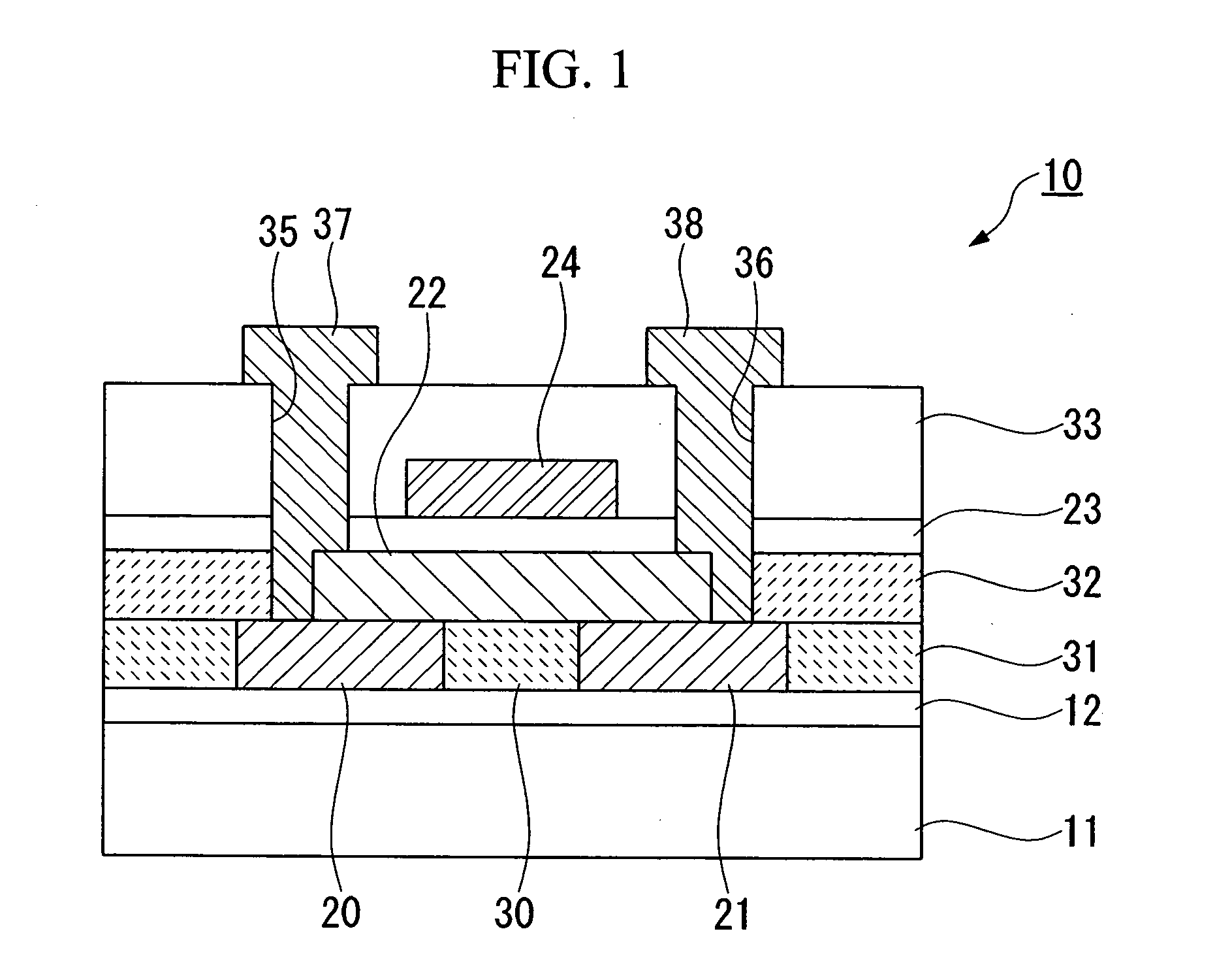
[0043]FIG. 1 is a typical cross-sectional view showing an example of an embodiment of the transistor according to the present invention. In FIG. 1, a backing insulating film 12 is formed on a substrate 11, and a transistor 10 that uses other crystalline silicon is formed on the substrate 11. The transistor 10 is provided with a source area 20 and a drain area 21 that are formed fro...


PUM


Abstract

There is provided a transistor and a method of manufacturing this transistor that allow a high degree of freedom when designing a wiring structure and also allow an improvement in product quality to be achieved. The transistor includes a source area, a drain area, and a channel area, each of which are formed by semiconductor films, and also a gate insulating film and a gate electrode. The semiconductor film containing the source area and the semiconductor film containing the drain area are formed separately sandwiching both sides of an insulating member. The semiconductor film containing the channel area is formed on top of the insulating member.

Description

BACKGROUND OF THE INVENTION [0001] 1. Field of the invention [0002] The present invention relates to a transistor that can be suitably used in an electro-optic device such as liquid crystal display device, an electroluminescent display device, and an electrophoretic display device as well as in an integrated circuit and to a method of manufacturing the transistor. The present invention also relates to an integrated circuit, an electro-optic device, and an electronic instrument that use this transistor. [0003] Priority is claimed on Japanese application No. 2002-351112, filed Dec. 3, 2002, the content of which is incorporated herein by reference. [0004] 2. Description of Related Art [0005] Generally, a transistor is formed by a source area, a drain area, and a channel area that are each formed by a semiconductor film, as well as a gate insulating film and a gate electrode. In a typical transistor structure a semiconductor film is formed by creating a source area, a drain area, and a ...

Claims


Application Information

Patent Timeline
IPC IPC(8): G02F1/1368H01L21/336H01L21/77H01L21/84H01L27/12H01L29/786
CPCH01L27/12H01L29/66757H01L29/66772H01L27/1292H01L29/78618H01L29/78636H01L29/78696H01L29/78603H01L29/786
Inventor YUDASAKA, ICHIOFURUSAWA, MASAHIROAOKI, TAKASHI
Owner SEIKO EPSON CORP
Why Eureka
Try Eureka