Display and method for driving the same

a technology of active matrix and display, applied in static indicating devices, instruments, non-linear optics, etc., to achieve the effect of reducing the amplitude of a video signal distributed to each signal line, eliminating spot defects caused by light leakage, and increasing the supply current to each pixel transistor

Inactive Publication Date: 2005-02-17
SONY CORP
View PDF5 Cites 21 Cited by
  • Summary
  • Abstract
  • Description
  • Claims
  • Application Information

AI Technical Summary

Benefits of technology

As mentioned above, the common electrodes of the auxiliary capacitors of the pixels are scanned row by row and the potential of each common electrode is changed, thus obtaining the following advantages. First, the amount of supply current to each pixel transistor is increased. Even when each auxiliary capacitance is increased, a spot defect is not generated by insufficient signal writing. Second, the amplitude of a video signal distributed to each signal line is reduced. Thus, a spot defect caused by light leak can be eliminated. Third, a variation in amplitude of a signal supplied to the signal line is little. Consequently, image quality defects such as longitudinal crosstalk, lateral crosstalk, a window strip depending on the amplitude can be eliminated. Fourth, the common electrodes of the auxiliary capacitors of the pixels are scanned row by row. Thus, the large amount of charge is not needed. High-speed scanning can be realized.

Problems solved by technology

These defects depend on the signal amplitude and are conventional problems.
Even when each auxiliary capacitance is increased, a spot defect is not generated by insufficient signal writing.

Method used


Image

  • Display and method for driving the same
  • Display and method for driving the same
  • Display and method for driving the same

Examples


Embodiment Construction

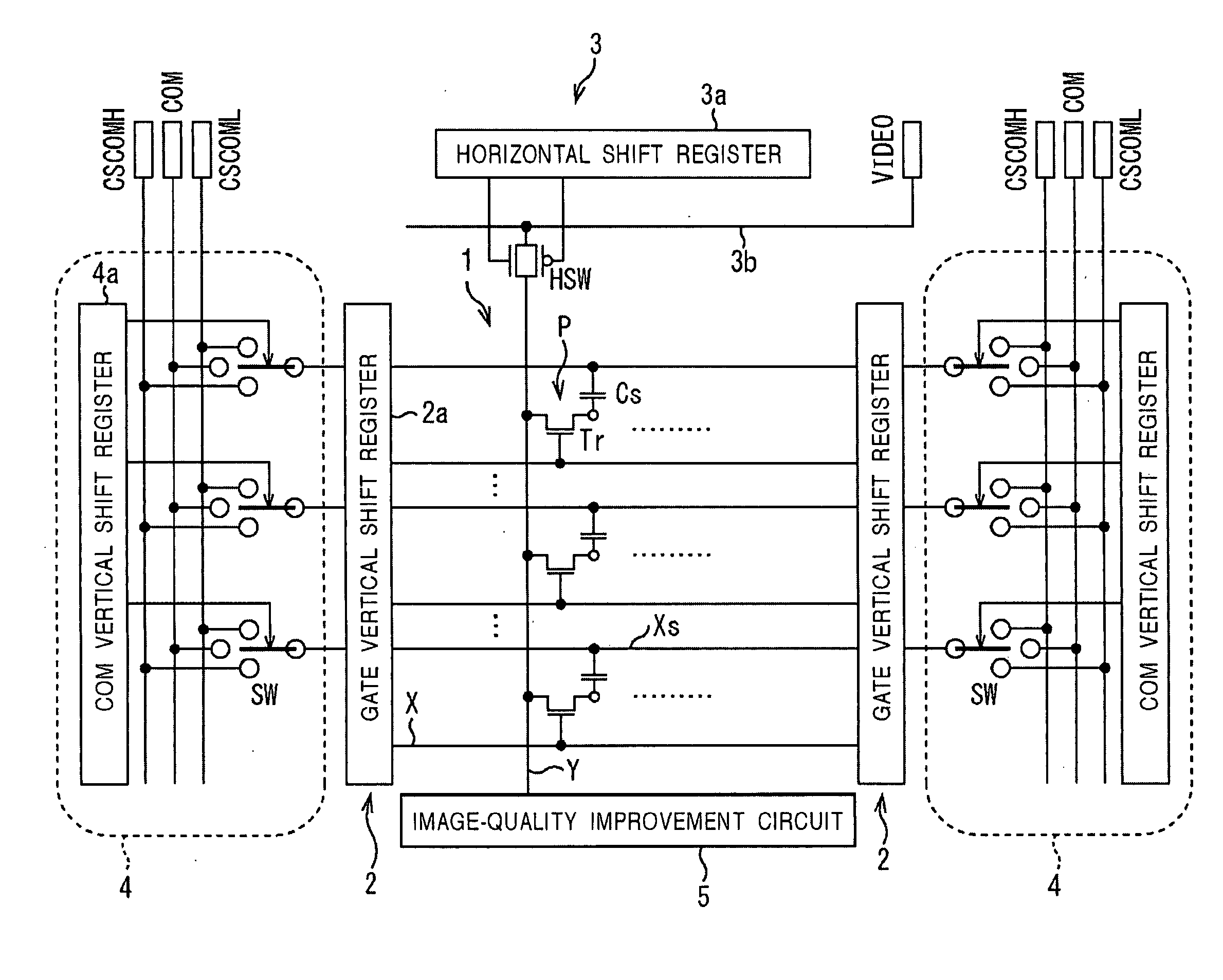
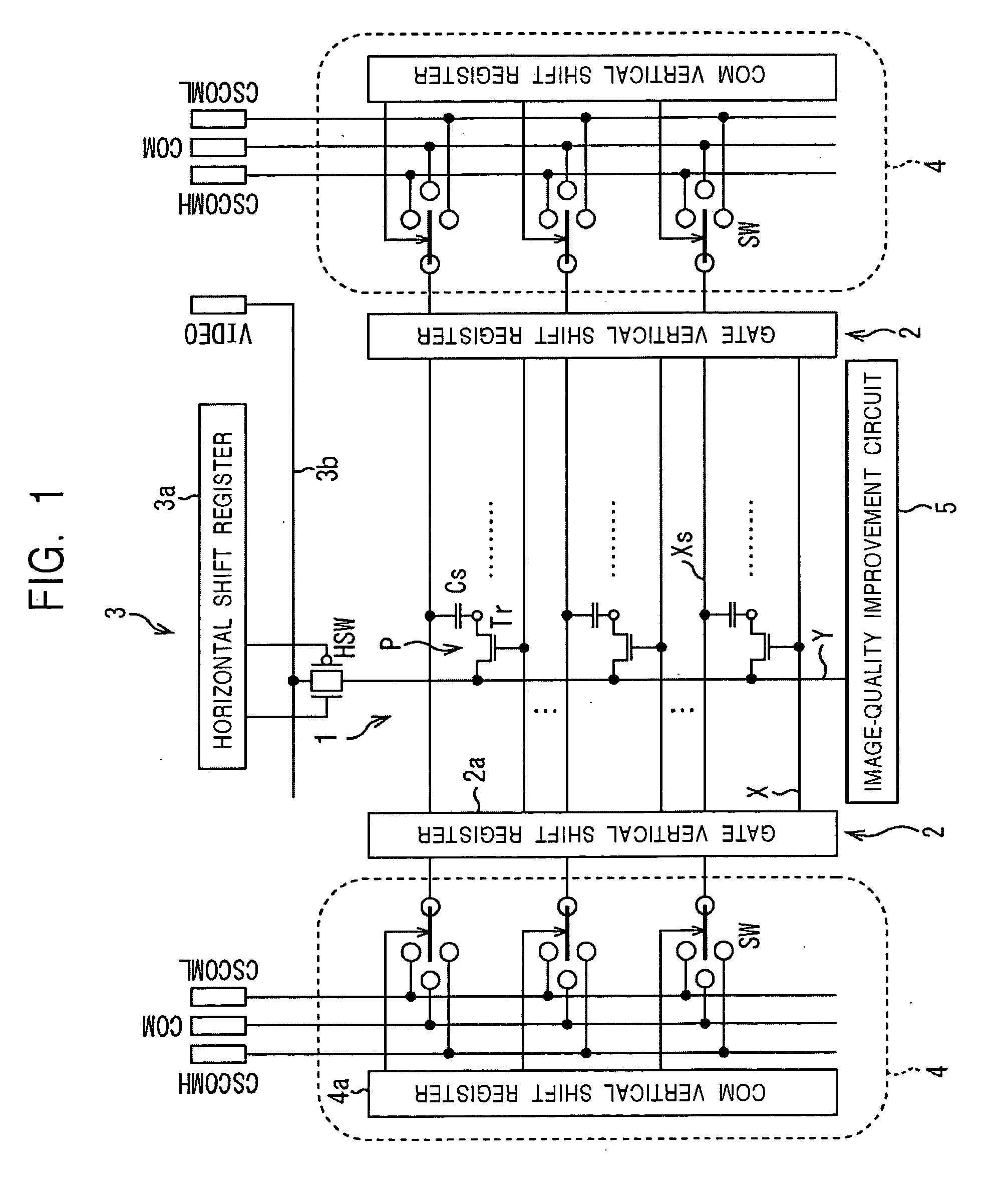
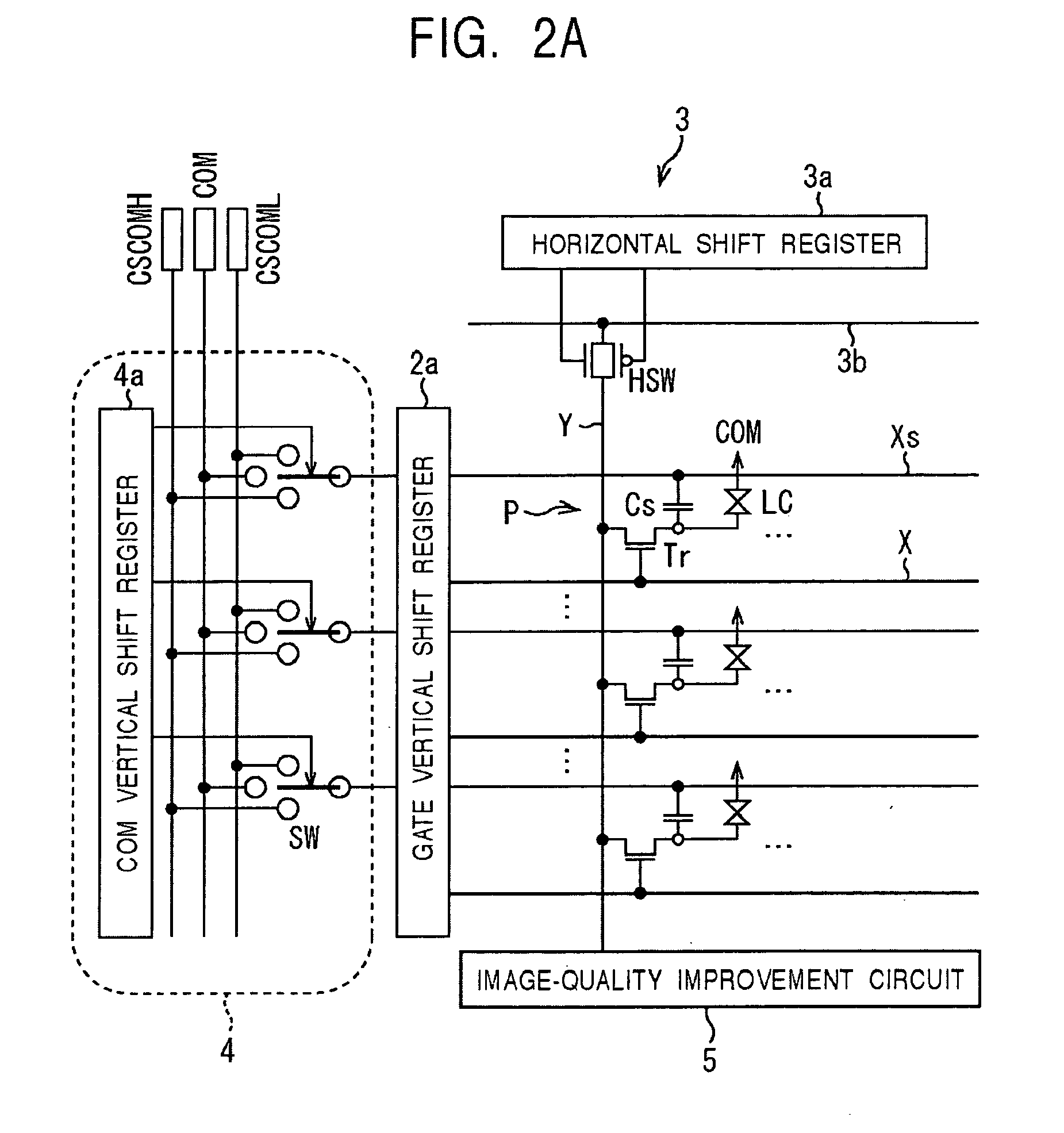
An embodiment of the present invention will now be described below in detail with reference to the drawings. FIG. 1 is a block diagram of the entire structure of a display according to the present invention.. The present display fundamentally includes a pixel array 1, a vertical scan circuit 2, a horizontal drive circuit 3, and an auxiliary scan circuit 4. The pixel array 1 includes scan lines x extending laterally, signal lines Y extending longitudinally, pixels P arranged in a matrix so as to correspond to the intersections of the scan lines X and the signal lines Y, and auxiliary scan lines Xs. The vertical scan circuit 2 includes one pair of gate vertical shift registers 2a arranged on the right and left sides of the pixel array 1 to simultaneously drive the pixel array 1 on both the sides. Specifically speaking, the vertical scan circuit 2 sequentially applies selection pulses to the scan lines X to sequentially the pixels P row by row.

The horizontal drive circuit 3 is arran...


PUM

PropertyMeasurementUnit
gate potentialaaaaaaaaaa
voltageaaaaaaaaaa

Abstract

A display includes a pixel array, a vertical scan circuit, a horizontal drive circuit, and an auxiliary scan circuit. The pixel array includes scan lines, signal lines, pixels, and auxiliary scan lines. Each pixel includes a transistor, a pixel electrode, and an auxiliary capacitor. The auxiliary scan circuit sequentially applies auxiliary pulses, of which potential is reversed between a high level and a low level relative to a predetermined reference potential, to the auxiliary scan lines synchronously with selection pulses to control such that a potential of one electrode of each auxiliary capacitor in a selected pixel row is opposite in polarity to that of a signal written in the corresponding pixel electrode in the selected row, and further control such that the potential of the electrode of each auxiliary capacitor is returned to the reference potential when the selected row is released.

Description

BACKGROUND OF THE INVENTION 1. Field of the Invention The present invention relates to an active matrix display, typified by an LCD, and a method for driving the display, and more particularly, relates to a technique for driving a transistor and an auxiliary capacitor formed in each pixel of a display. 2. Description of the Related Art FIG. 17 is a block diagram of a conventional display. The display includes a pixel array 1, a pair of vertical shift registers 2a, and a horizontal shift register 3a. The pixel array 1 includes scan lines X extending laterally, signal lines Y extending longitudinally, pixels P arranged in a matrix so as to correspond to the respective intersections of the scan lines X and the signal lines Y, and auxiliary capacitor lines Xs arranged parallel to the scan lines X. The vertical shift registers 2a are arranged on the right and left sides of the pixel array 1 to simultaneously drive the pixel array 1 on both the sides. In other words, each vertical shif...

Claims


Application Information

Patent Timeline
Patent Type & Authority Applications(United States)
IPC IPC(8): G02F1/1368G02F1/133G09G3/20G09G3/36
CPCG09G2320/02G09G3/3655G09G3/36
Inventor NODA, KAZUHIRO
Owner SONY CORP
Why Eureka
Try Eureka