[0009]The present invention has been proposed to solve the above-mentioned problems. An object of the present invention is to provide a
semiconductor chip, which has such a structure capable of reducing the carrier
life time as compared with the conventional techniques, a method of manufacturing the semiconductor
chip, a terahertz electromagnetic-wave device to which the semiconductor chip is applied, and a method of manufacturing the terahertz electromagnetic-wave device.
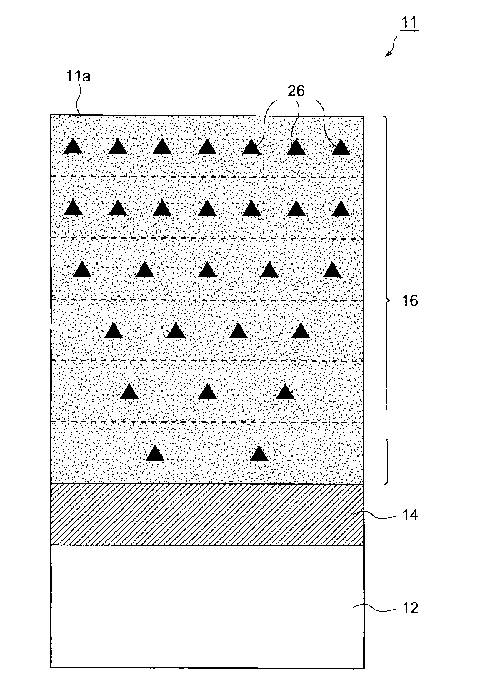
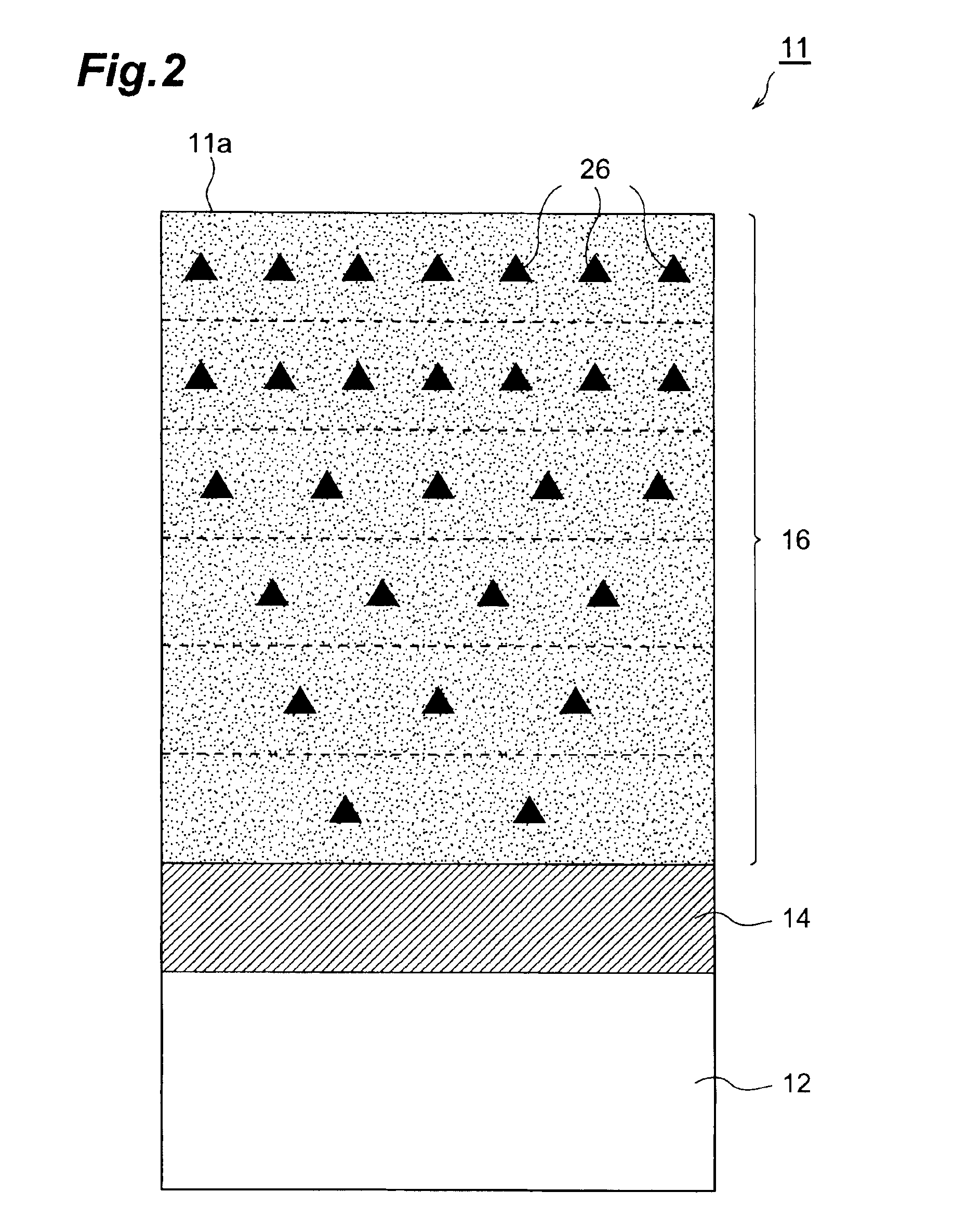
[0012]As described above, in this semiconductor chip, the concentration of Group V atoms in the second main surface side of the Group III-V compound semiconductor layer is set higher than the concentration of the Group III atoms. Therefore, in the vicinity of the upper surface (second main surface) of the Group III-V compound semiconductor layer, many clusters of Group V atoms are deposited. It is known that these Group V atom clusters function as a main factor of the
carrier capture. Specifically, it is known that the Group V atom clusters in the vicinity of the upper surface of the Group III-V compound semiconductor layer contribute largely to the
carrier capture. Further, the Group III-V compound semiconductor layer includes the oxygen, and a
deep level is formed due to the included oxygen. And the fact that the
deep level formed by the oxygen contributes the reduction of the life of the carriers has been found by the inventors. Based on the above-mentioned facts, the semiconductor chip according to the present invention is capable of further reducing the life of the carriers.
[0014]In this way, in the second main surface side of the semiconductor chip, the concentration of the Group V atoms of the Group III-V compound semiconductor layer is higher than the concentration of the Group III atoms. Accordingly, many clusters of the Group V atoms are deposited in the vicinity of upper surface (second main surface) of the Group III-V compound semiconductor layer. Also, in the Group III-V compound semiconductor layer, from the first main surface toward the second main surface, the ratio of the concentration of the Group V atoms with respect to the concentration of the Group III atoms increases. Accordingly, the ratio of the concentration in the first main surface side (a portion closer to the above-mentioned
single crystal semiconductor substrate) in the Group III-V compound semiconductor layer is reduced to a certain low level. Owing to this, the uniformity of the
crystal in the first main surface side of the Group III-V compound semiconductor layer is high. Thus, the semiconductor chip according to the present invention enables to further reduce the life of the carriers as well as the uniformity of the
crystal in the first main surface side of the Group III-V compound semiconductor layer is ensured.
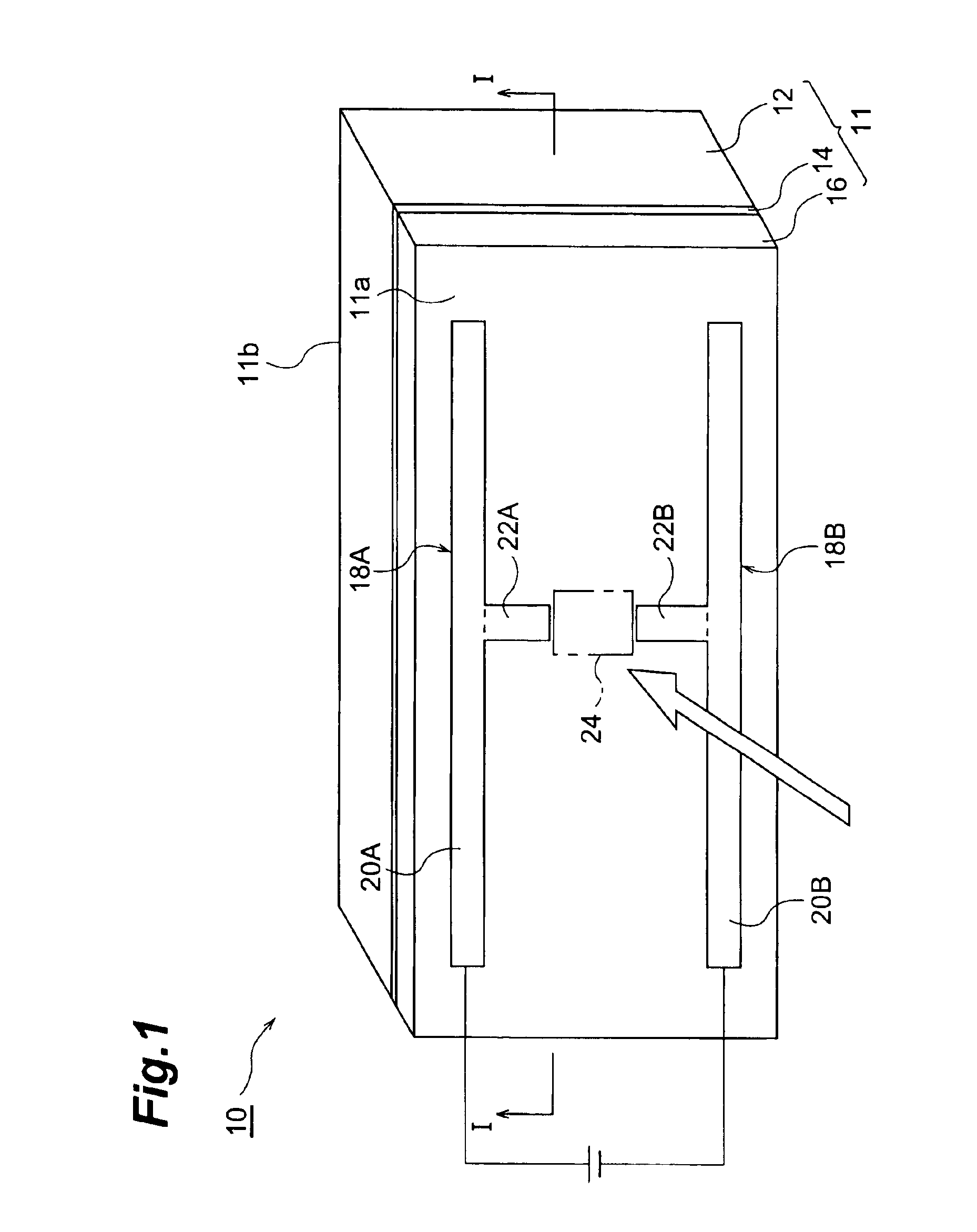
[0019]In this way, in the terahertz electromagnetic-wave device, also in such a constitution that the concentration of the Group V atoms is higher than the concentration of the Group III atoms in the second main surface side of the Group III-V compound semiconductor layer, many clusters of the Group V atoms are deposited in the vicinity of the upper surface (second main surface) of the Group III-V compound semiconductor layer. Thus, in the terahertz electromagnetic-wave device, owing to such constitution that the clusters of the Group V atoms in the vicinity of the upper surface of the Group III-V compound semiconductor layer increase significantly, the life of the carriers can be further reduced. Accordingly, in the terahertz electromagnetic-wave device according to the present invention, a high-speed response can be achieved when the minute gap between the pair of antenna electrodes is irradiated with
femtosecond laser. Further, the Group III-V compound semiconductor layer is arranged so that the ratio of the concentration of the Group V atoms with respect to the concentration of the Group III atoms increases from the first main surface toward the second main surface. Accordingly, in the first main surface side (in a portion closer to the
single crystal semiconductor substrate) of the Group III-V compound semiconductor layer, the concentration rate is reduced to a certain level. Accordingly, the uniformity of the
crystal in the first main surface side of the Group III-V compound semiconductor layer is increased.
[0021]Further, in the
meth of manufacturing the semiconductor chip according to the present invention, the epitaxial growth for forming the Group III-V compound semiconductor layer directly or indirectly on the single crystal semiconductor substrate may be carried out while increasing the supply amount of Group V material and lowering the substrate temperature. In this way, it is arranged so that, in the second main surface side of the obtained Group III-V compound semiconductor layer, the concentration of the Group V atoms is higher than the concentration of the Group III atoms as well as the ratio of the concentration of the Group V atoms with respect to the concentration of the Group III atoms increases from the first main surface toward the second main surface.
[0023]Further, in the method of manufacturing the terahertz electromagnetic-wave device according to the present invention, the epitaxial growth for forming the Group III-V compound semiconductor layer directly or indirectly on the single crystal semiconductor substrate may be carried out while increasing the supply amount of Group V material and lowering the substrate temperature. In this way, it is arranged so that, in the second main surface side of the obtained Group III-V compound semiconductor layer, the concentration of the Group V atoms in is higher than the concentration of the Group III atoms as well as the ratio of the concentration of the Group V atoms with respect to the concentration of the Group III atoms increases from the first main surface toward the second main surface.

