Protection of conductors from oxidation in deposition chambers

a technology of conductors and deposition chambers, which is applied in the direction of chemical vapor deposition coatings, electrical equipment, coatings, etc., can solve the problems of complex process of semiconductor device fabrication, and achieve the effect of reducing the temperature of the substrate and increasing the pressure in the cvd chamber

Active Publication Date: 2010-08-26
ASM INTERNATIONAL
View PDF41 Cites 2 Cited by
  • Summary
  • Abstract
  • Description
  • Claims
  • Application Information

AI Technical Summary

Benefits of technology

[0007]According to some embodiments of the invention, a method for producing a transition metal nitride film is provided. A substrate is provided in a chemical vapor deposition (CVD) chamber. A transition metal nitride film is deposited on the substrate in the CVD chamber at a deposition pressure and a deposition temperature. Subsequently, the pressure in the CVD chamber is increased from the deposition pressure to an unloading pressure by flowing a reducing gas into the CVD chamber. The reducing gas comprises an inert gas and a reducing agent. While increasing the pressure in the CVD chamber, the temperature of the substrate is reduced from the deposition temperature to an unloading temperature. The substrate is unloaded from the CVD chamber at the unloading pressure and the unloading temperature.
[0008]According to other embodiments of the invention, a method for semiconductor processing is provided. A substrate is provided in a deposition chamber. A conductive film is deposited on the substrate in the chamber at a deposition pressure. The pressure in the CVD chamber is subsequently increased from the deposition pressure to an unloading pressure by flowing a reducing gas into the CVD chamber. The reducing gas comprises an inert gas and a reducing agent. The amount of the reducing agent in the chamber is smaller than the amount of the inert gas. The substrate is unloaded from the chamber at the unloading pressure.

Problems solved by technology

Semiconductor device fabrication is a complex process.

Method used


Image

  • Protection of conductors from oxidation in deposition chambers
  • Protection of conductors from oxidation in deposition chambers
  • Protection of conductors from oxidation in deposition chambers

Examples


example

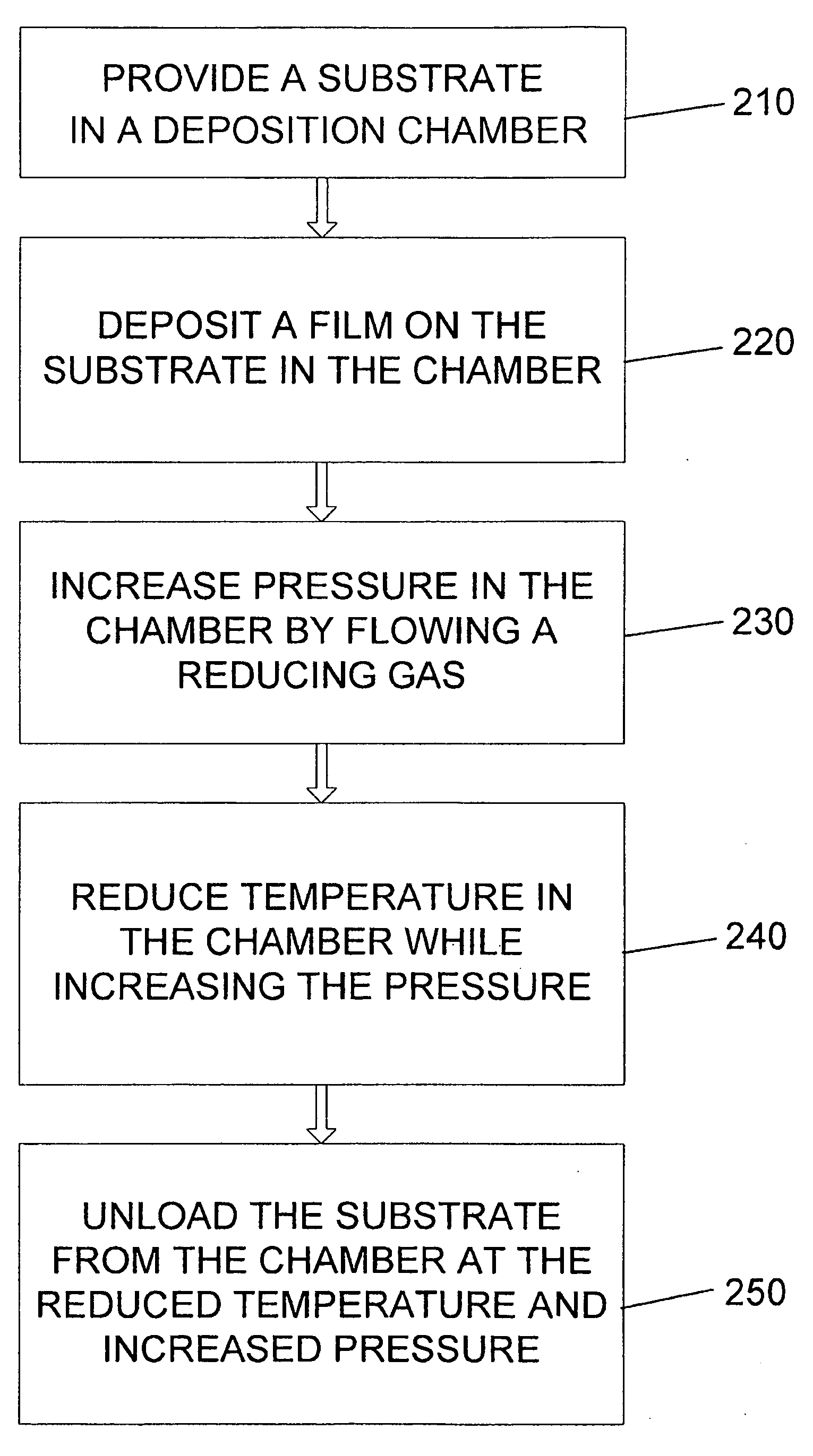
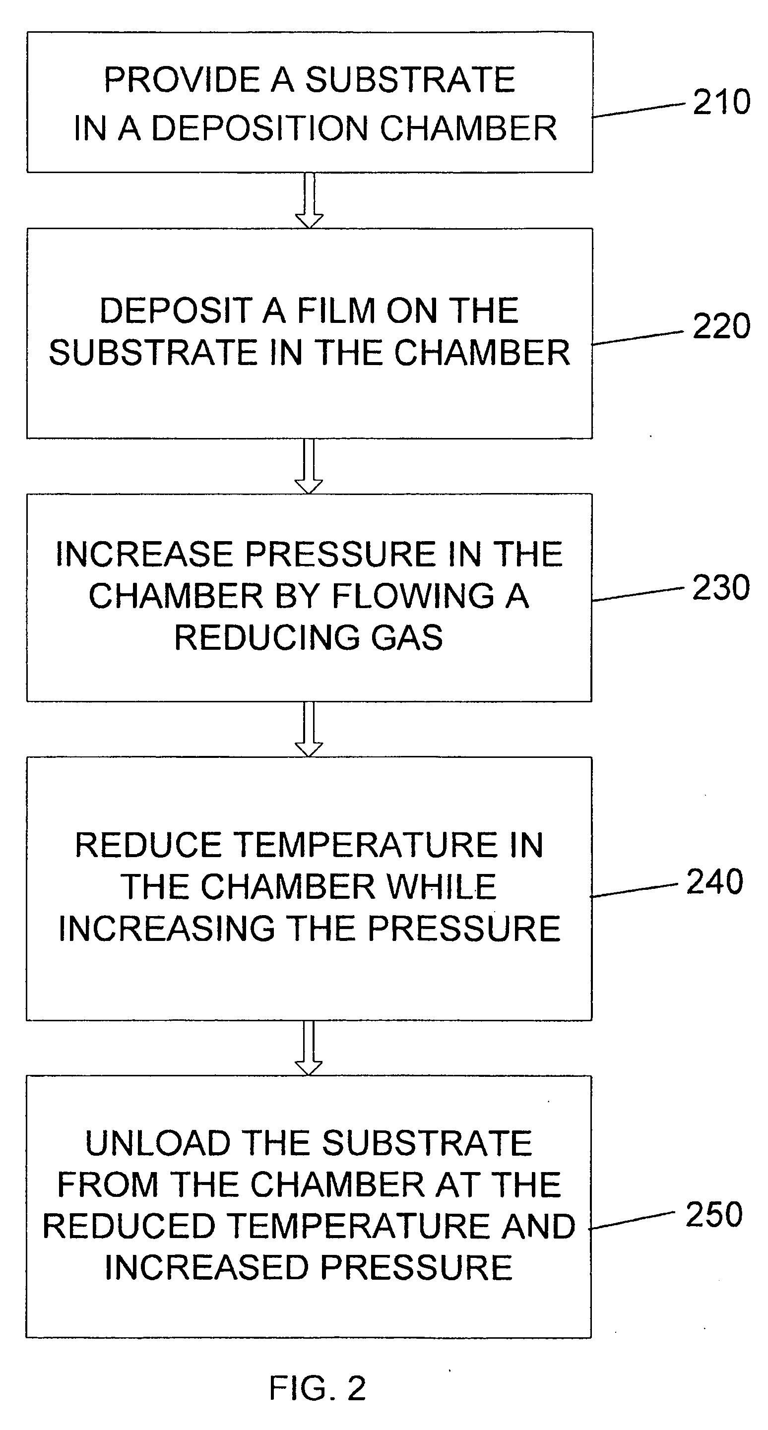
[0041]The resistivities of titanium nitride films produced under various conditions were analyzed. Titanium nitride films were deposited on substrates in an A412™ CVD batch reactor commercially available from ASM International, N.V. of Almere, the Netherlands. The titanium nitride was deposited by chemical vapor deposition using TiCl4 and NH3 at flow rates of about 2 g / min and 0.2 slm, respectively. The deposition temperature was about 600° C., and the deposition pressure was about 0.2 Torr. Under these conditions, the depositions processes were performed for various durations, resulting in the deposition of titanium nitride films having thicknesses of 10 nm, 20 nm, and 40 nm. The deposited films were subjected to various post-deposition processes and the resistivities of the films were measured, the results of which are presented in FIG. 4.

[0042]In all cases, the post-deposition processes included backfilling the deposition chamber to increase the pressure in the chamber to about a...


PUM

PropertyMeasurementUnit
pressureaaaaaaaaaa
pressureaaaaaaaaaa
temperatureaaaaaaaaaa

Abstract

In some embodiments, after depositing conductive material on substrates in a deposition chamber, a reducing gas is introduced into as the chamber in preparation for unloading the substrates. The deposition chamber can be a batch CVD chamber and the deposited material can be a metal nitride, e.g., a transition metal nitride such as titanium metal nitride. As part of the preparation for unloading substrates from the chamber, the substrates may be cooled and the chamber is backfilled with a reducing gas to increase the chamber pressure. It has been found that oxidants can be introduced into the chamber during this time. The introduction of a reducing gas has been found to protect exposed metal-containing films from oxidation during the backfill and/or cooling process. The reducing gas is formed of a reducing agent and a carrier gas, with the reducing agent being a minority component of the reducing gas. By providing a reducing agent, the effects of oxidation on exposed metal-containing films is reduced, therefore enhancing the conductive properties of the metal films.

Description

BACKGROUND[0001]1. Field of the Invention[0002]This application relates generally to semiconductor fabrication and, more particularly, to preventing post-deposition oxidation of metal-containing films.[0003]2. Description of the Related Art[0004]Semiconductor device fabrication is a complex process. Electronic devices are typically formed on a semiconductor substrate, and often include conductive elements separated by insulating elements. Conductive elements may serve as, e.g., electrodes and interconnecting conductors.[0005]Various electronic devices, such as transistor devices, exist in the modern day fabrication of integrated circuits, with metal-oxide-semiconductor field-effect transistors (MOSFET) being a common transistor device. Generally, a MOSFET includes a conductive gate electrode formed over a gate dielectric, which in turn overlies a semiconductor substrate that is typically single-crystal silicon. For reliable performance in electronic devices, such as a MOSFET, it is ...

Claims


Application Information

Patent Timeline
Patent Type & Authority Applications(United States)
IPC IPC(8): H01L21/285
CPCC23C16/34H01L21/76841H01L21/28556C23C16/56
Inventor YOSHIMI, TATSUYADE BLANK, RENENOIRAY, JEROME
Owner ASM INTERNATIONAL
Why Eureka
Try Eureka