Focal point detection device and camera
a technology of point detection device and camera, which is applied in the direction of camera focusing arrangement, exposure control, printers, etc., can solve the problems of camera not being provided as a compact unit, image cannot always be obtained at an image-capturing element, and potential adjustment errors
- Summary
- Abstract
- Description
- Claims
- Application Information
AI Technical Summary
Benefits of technology
Problems solved by technology
Method used
Image

Examples
first embodiment
[0063] -First Embodiment-
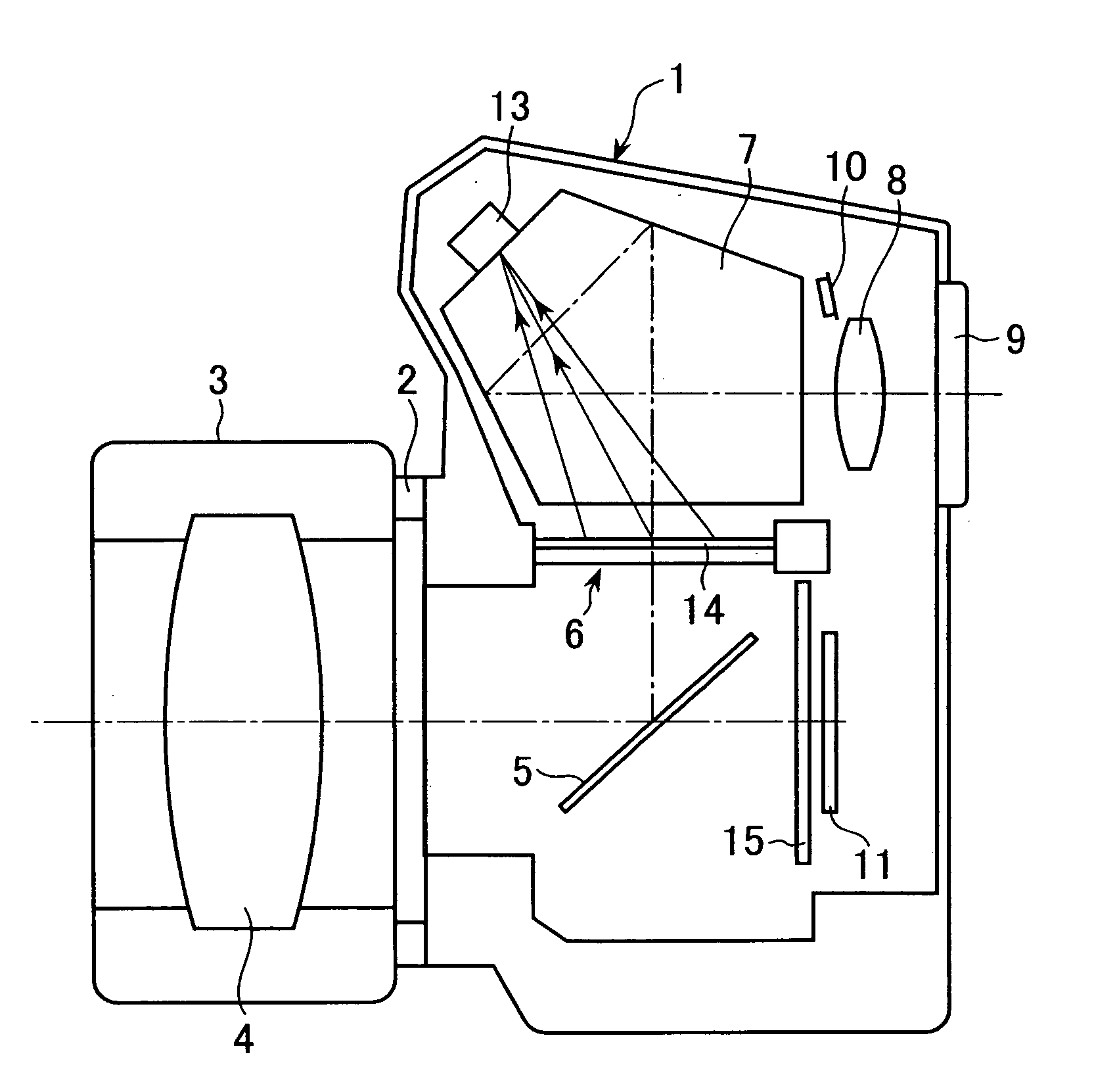
[0064]FIG. 1 shows a camera achieved in an embodiment of the present invention in a schematic sectional view of a single lens reflex digital camera. A lens barrel 3 is mounted at a lens mount 2 of the camera 1. Subject light having passed through a photographic optical system 4 disposed in the lens barrel 3 is reflected at a quick return mirror 5 and forms an image on a liquid crystal optical member 6. The liquid crystal optical member 6 is disposed at a position optically equivalent to an estimated image forming plane of the photographic optical system 4, in the vicinity of a position at which a view finder screen should be set. In this embodiment, an image-capturing element 11 is disposed at the estimated image forming plane of the photographic optical system 4, and the liquid crystal optical member 6 also functions as the viewfinder screen. The image-capturing element 11 is a two-dimensional image-capturing device which maybe a CCD-type, a MOS-type or a C...
second embodiment -
[0130] -Second Embodiment-
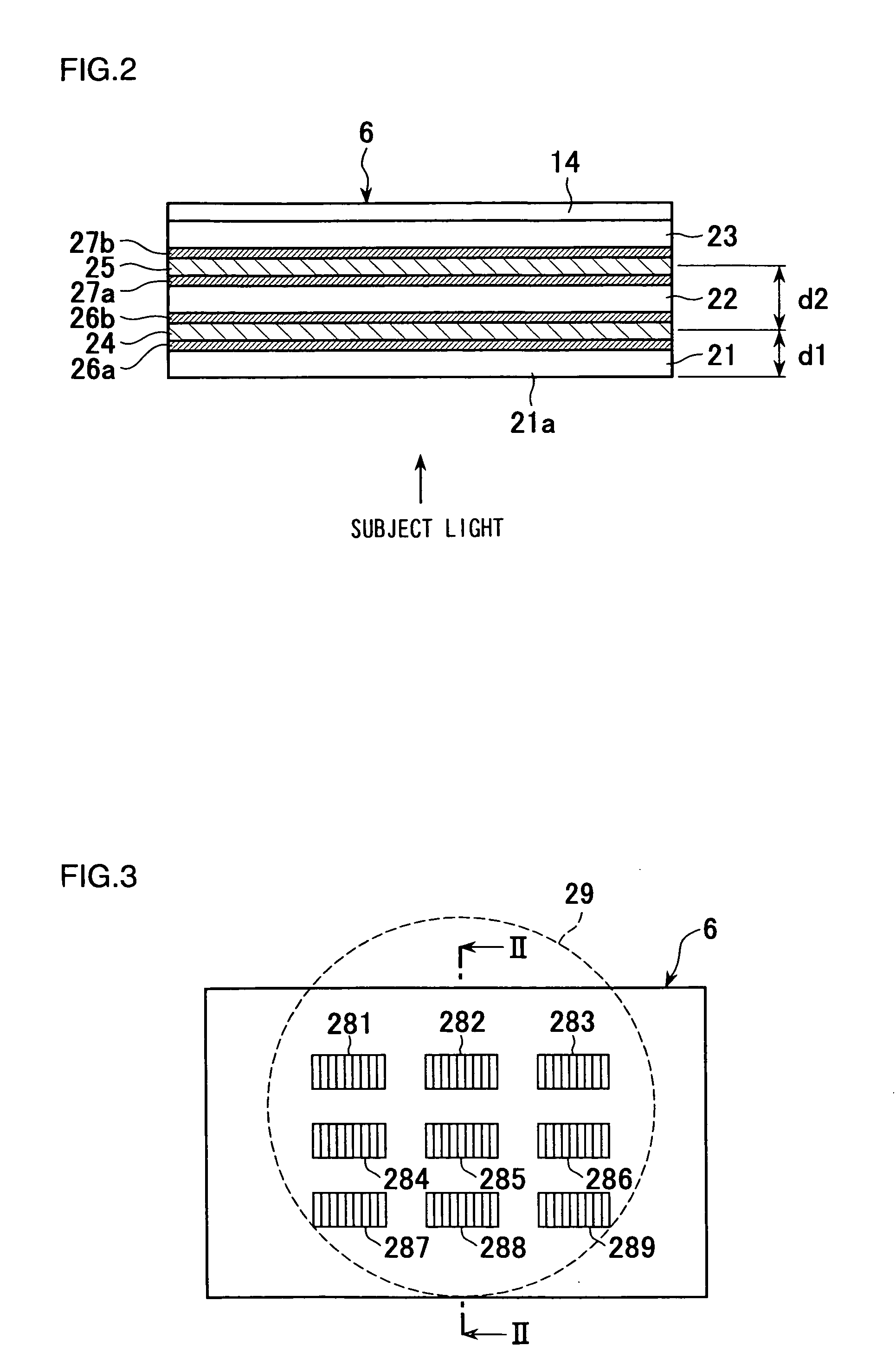
[0131] In the first embodiment described above, the surfaces of the detection areas 281 to 289 at the condenser optical element 14 have a contour identical to the surface contour of the lens 29, as shown in FIGS. 3 and 4, to condense light passing through the detection areas 281 to 289. In the second embodiment, a condenser optical element 140 constituted of an optically anisotropic liquid crystal and a transparent isotropic polymer is used instead of the condenser optical element 14 described above. The condenser optical element 140, which functions as a diffraction grating, adopts a structure shown in the sectional view in FIG. 18. FIG. 18 is a schematic sectional view of the detection area 285 at the condenser optical element 140, taken along the horizontal direction in FIG. 3.
[0132] Reference numerals 141 and 142 in FIG. 18 each indicate a glass substrate, and electrode patterns are formed with transparent conductive films 143 and 144 at the surfaces o...
third embodiment
[0154] -Third Embodiment-
[0155]FIG. 26 is a block diagram similar to that presented in FIG. 24, showing the AF system achieved in the third embodiment of the present invention. It is to be noted that the same reference numerals are assigned to components identical to those in the second embodiment, and the following explanation focuses on the differences. Reference numeral 60 in FIG. 26 indicates a liquid crystal optical member having a filter F1 and a filter F12. As detailed later, the filter F12 in the third embodiment has the function of the filter 2 and the function of the condenser optical element 140 in FIG. 24. The distance between the filter F1 and the viewfinder screen 21a is set to d1, and the distance between the filter F1 and the filter F12 is set to d2. The operation of the filter F12 is controlled by a filter control unit 61.
[0156]FIG. 27 is a sectional view of the liquid crystal optical member 60, and FIG. 28 is a plan view of the liquid crystal optical member 60. Th...
PUM
 Abstract
Description
Claims
Application Information
 - R&D Engineer
- R&D Manager
- IP Professional
- Industry Leading Data Capabilities
- Powerful AI technology
- Patent DNA Extraction
Browse by: Latest US Patents, China's latest patents, Technical Efficacy Thesaurus, Application Domain, Technology Topic.
© 2024 PatSnap. All rights reserved.Legal|Privacy policy|Modern Slavery Act Transparency Statement|Sitemap