In-line spectroscopy for process monitoring

a technology of in-line spectroscopy and process monitoring, which is applied in the direction of fluorescence/phosphorescence, optical radiation measurement, instruments, etc., can solve the problems of high wafer cost, high overall density, and damage to the intended function of these dielectrics

Inactive Publication Date: 2005-02-17
C I SYST ISRAEL
View PDF2 Cites 30 Cited by
  • Summary
  • Abstract
  • Description
  • Claims
  • Application Information

AI Technical Summary

Benefits of technology

Recently, compact Raman probeheads, for illuminating a sample with laser radiation and for collecting the Raman spectrum from the sample after filtering out the directly scattered laser radiation, have become available. One such Raman probehead is the Mark II Filtered Probehead, available from Kaiser Optical Systems, Inc. of An Arbor Mich. USA. Another such Raman probehead is the probehead of the RP-1 spectrograph, available from SpectraCode of West Lafayette Ind. USA. These probeheads have been used for applications other than in-line monitoring of industrial processes. For example, the RP-1 spectrograph is advertised as suitable for “point and shoot” identification of polymer resins. The present invention is based on the realization that these probeheads can indeed be used for in-line monitoring of industrial processes such as the application of a low-K dielectric layer to a silicon wafer and the subsequent annealing or curing of the layer.

Problems solved by technology

Many of these materials are manufactured with added porosity in their bulk, to reduce their overall density, and are hygroscopic.
As a result, moisture uptake from the environment, which is detrimental to the intended function of these dielectrics, must be controlled.
In view of the high wafer costs, these from the production line for off-line testing cannot be used for the final product, and must be discarded.
Second, by the time the results of the test are known and analyzed, many other wafers have gone through the production processes.
These wafers may have the same unsuitable characteristics as the tested wafer, and so must be scrapped.
Note that the relevant Raman spectra heretofore have been measured using research-grade Raman spectrographs, which are not suitable for use in the environment of an industrial production line, and in particular are not suitable for in-line monitoring of semiconductor wafers in a fab.
As noted above, many low-K materials, and in particular porous low-K materials, tend to be hygroscopic.

Method used


Image

  • In-line spectroscopy for process monitoring
  • In-line spectroscopy for process monitoring
  • In-line spectroscopy for process monitoring

Examples


Embodiment Construction

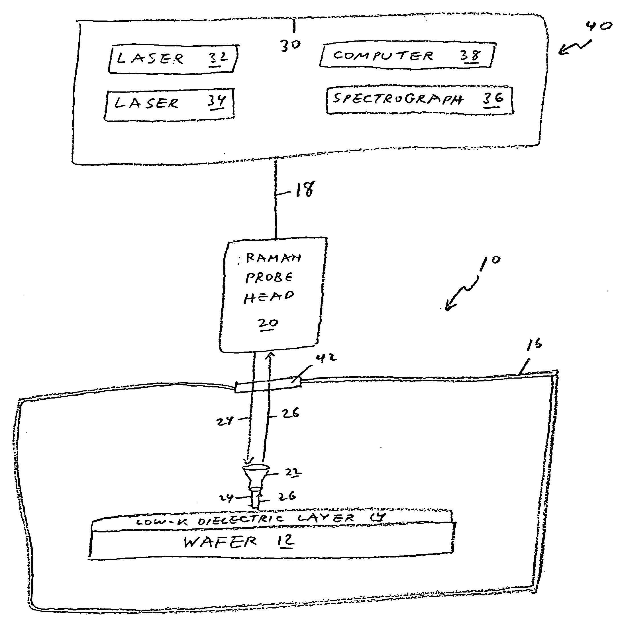
The present invention is of a method of processing a workpiece, while monitoring the processing using an optical excitation technique such as Raman scattering. The monitoring of the present invention may be simultaneous with or subsequent to the processing, in the same chamber or in a different chamber. Specifically, the present invention can be used to deposit and anneal or cure a layer of low-K dielectric on a semiconductor wafer.

The principles and operation of workpiece processing according to the present invention may be better understood with reference to the drawings and the accompanying description.

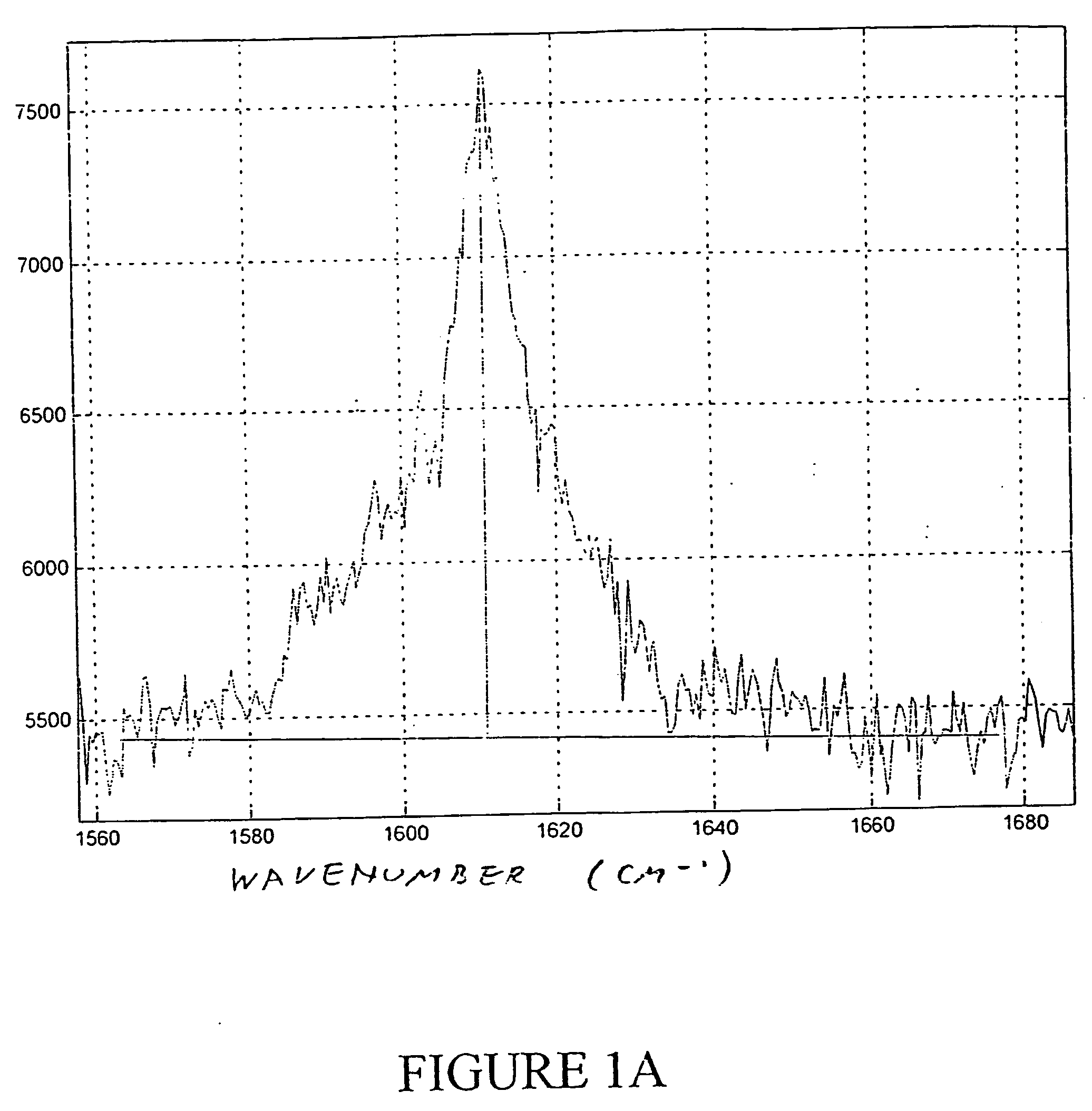
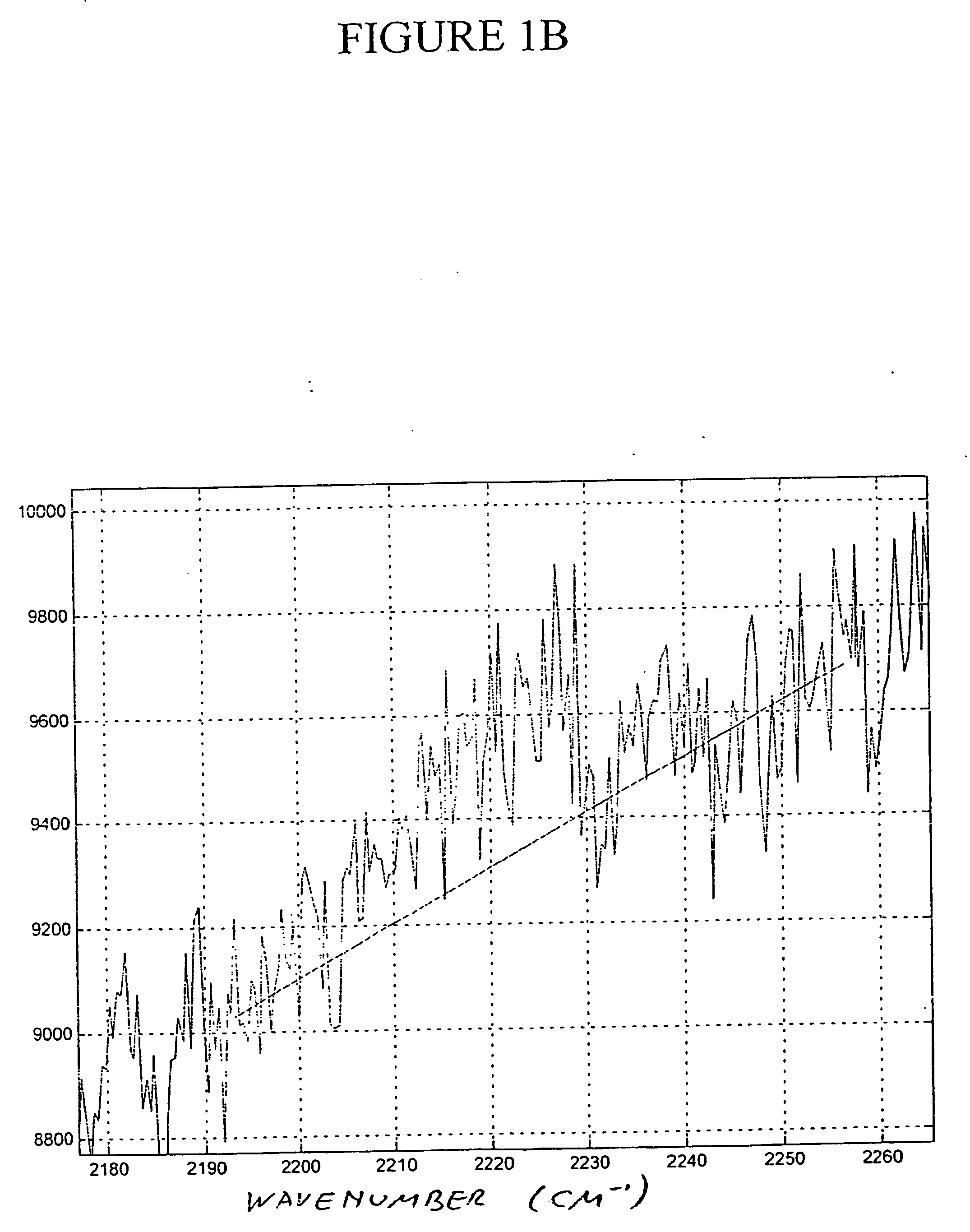
We have performed our own Raman spectral measurements of properties of interest in low-K dielectrics on silicon wafers. Referring now to the drawings, FIGS. 1A through 10 illustrate some of these measurements.

1. Curing of SiLK™

SiLK™ is a low-K dielectric material that is manufactured and sold by Dow Chemical Company of Midland Mich. USA. FIGS. 1A and 1B are portions of a Ram...


PUM

PropertyMeasurementUnit
feature sizesaaaaaaaaaa
wavenumbersaaaaaaaaaa

Abstract

A method for processing a workpiece and an associated processing chamber and analytic instrument. A layer of a material such as a low-K dielectric is applied to a workpiece such as a semiconductor wafer. During the application, and/or before or during subsequent processing, a property of the layer is measured by steps including exciting a portion of the layer with incident light and monitoring light such as Raman scattered light that is emitted from that portion of the layer in response to the incident light, via a probehead that may be inside or outside the chamber housing. The analytic instrument includes the probehead and two sources of excitation light at two different wavelengths.

Description

FIELD AND BACKGROUND OF THE INVENTION The present invention relates to in-line monitoring of a workpiece undergoing processing and, more particularly, to in-line monitoring of a workpiece, such as a semiconductor wafer to which a layer of low-K dielectric is applied, using Raman spectroscopy. The semiconductor industry is gradually introducing new dielectric materials as electrical insulators of-integrated circuits, instead of SiO2. These materials, so called low-K dielectrics, have lower dielectric constants than SiO2. This change is driven by the constant reduction of the size of the smallest features on a chip, and by the adoption of copper as the metal used for the electrical connections, instead of aluminum. These new dielectric materials must comply with a long list of very stringent requirements, with respect to their physical and chemical properties. These requirements include high mechanical stability, good adhesion to the substrate, the ability to withstand thermal stres...

Claims


Application Information

Patent Timeline
Patent Type & Authority Applications(United States)
IPC IPC(8): G01J3/44G01N21/21G01N21/64G01N21/65G01N21/95
CPCG01J3/44G01N21/211G01N21/64G01N2021/8427G01N21/9501G01N2021/656G01N21/65
Inventor CABIB, DARIOBUCKWALD, ROBERT A.
Owner C I SYST ISRAEL
Why Eureka
Try Eureka