Plasma display panel and manufacturing method
- Summary
- Abstract
- Description
- Claims
- Application Information
AI Technical Summary
Benefits of technology
Problems solved by technology
Method used
Image

Examples
first embodiment
[0057] First Embodiment
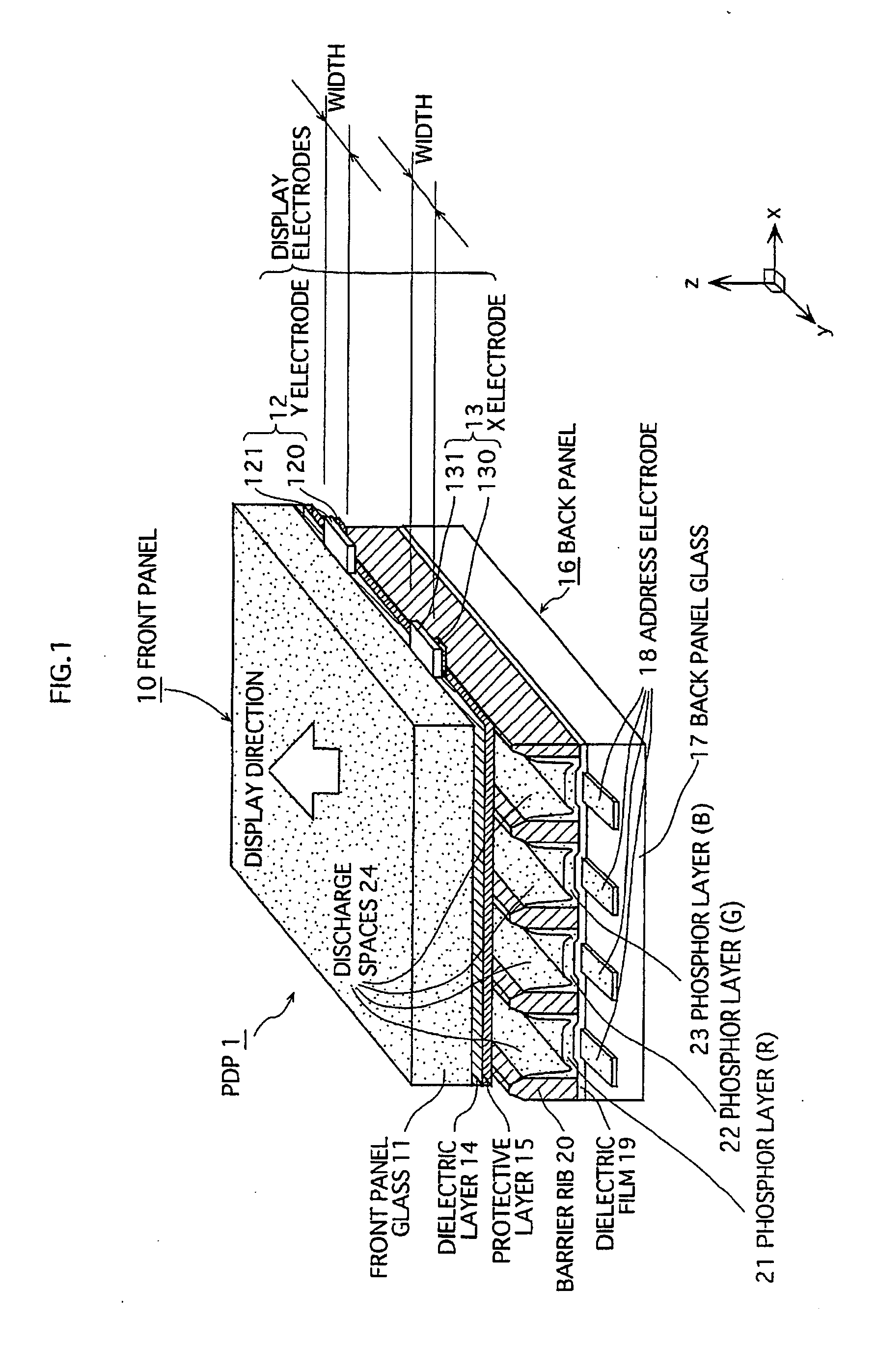
[0058] [1.1 Construction of a PDP]
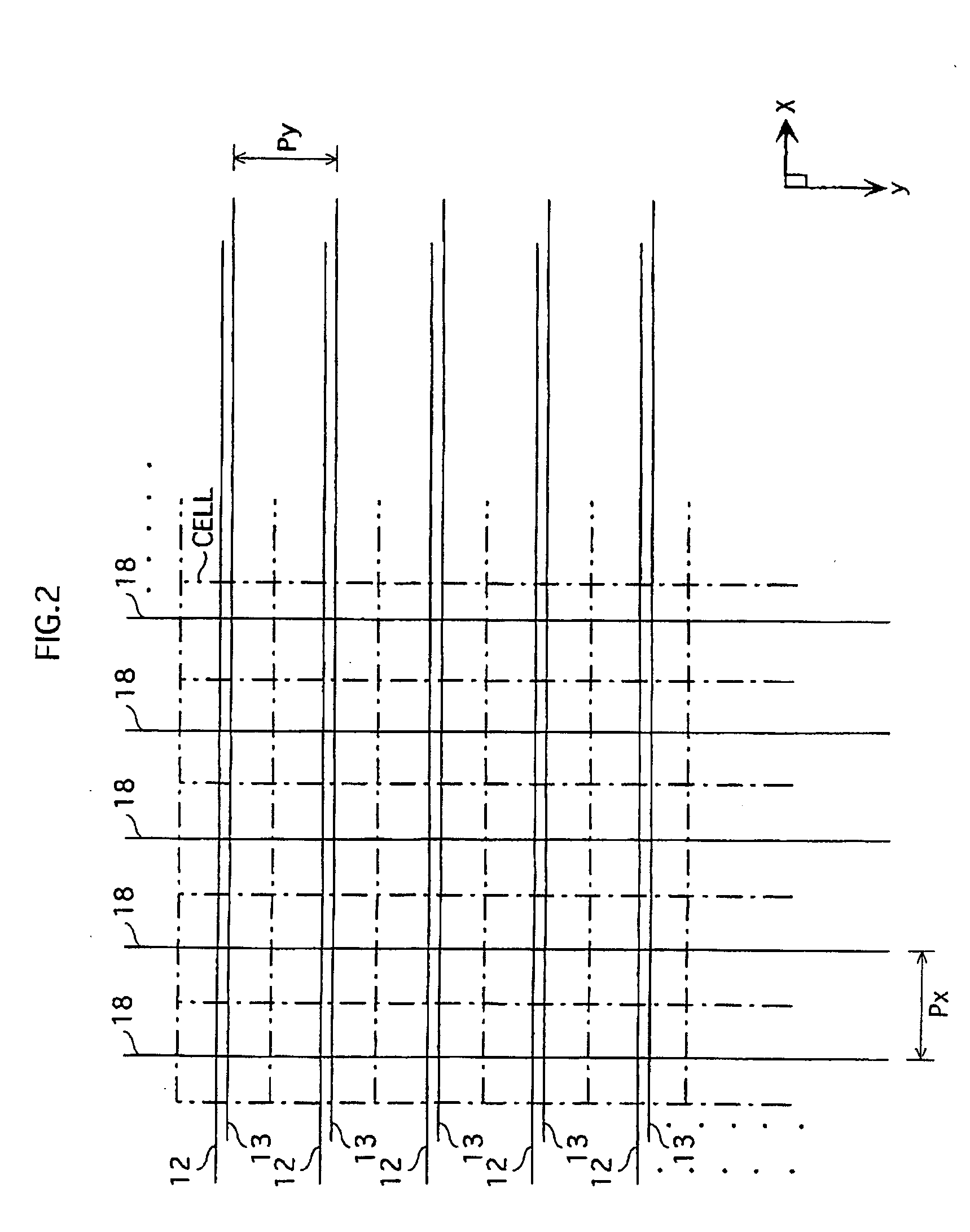
[0059]FIG. 3 is a schematic view showing an arrangement of the display electrodes 12 and 13 and the address electrodes 18 in the PDP 1 relating to a first embodiment. Here, FIG. 3 is a plan view showing a plane parallel to the xy plane in FIG. 1. In FIG. 3, Px indicates a pitch of the address electrodes 18 that are arranged so as to be adjacent to each other in the horizontal (x) direction of the panel. Py indicates a pitch of the display electrodes 12 or 13 that are arranged so as to be adjacent to each other in the vertical (y) direction of the panel. Py is hereinafter referred to as a display electrode pitch. The display electrodes 12 and 13 have a laminated construction including a transparent electrode and a bus line as described before, but they are schematically indicated by straight lines in FIG. 3.
[0060] In all of the following embodiments, the x direction and the y direction represent the row direction and the colum...
second embodiment
[0107] Second Embodiment
[0108] [2.1. Construction of the PDP]
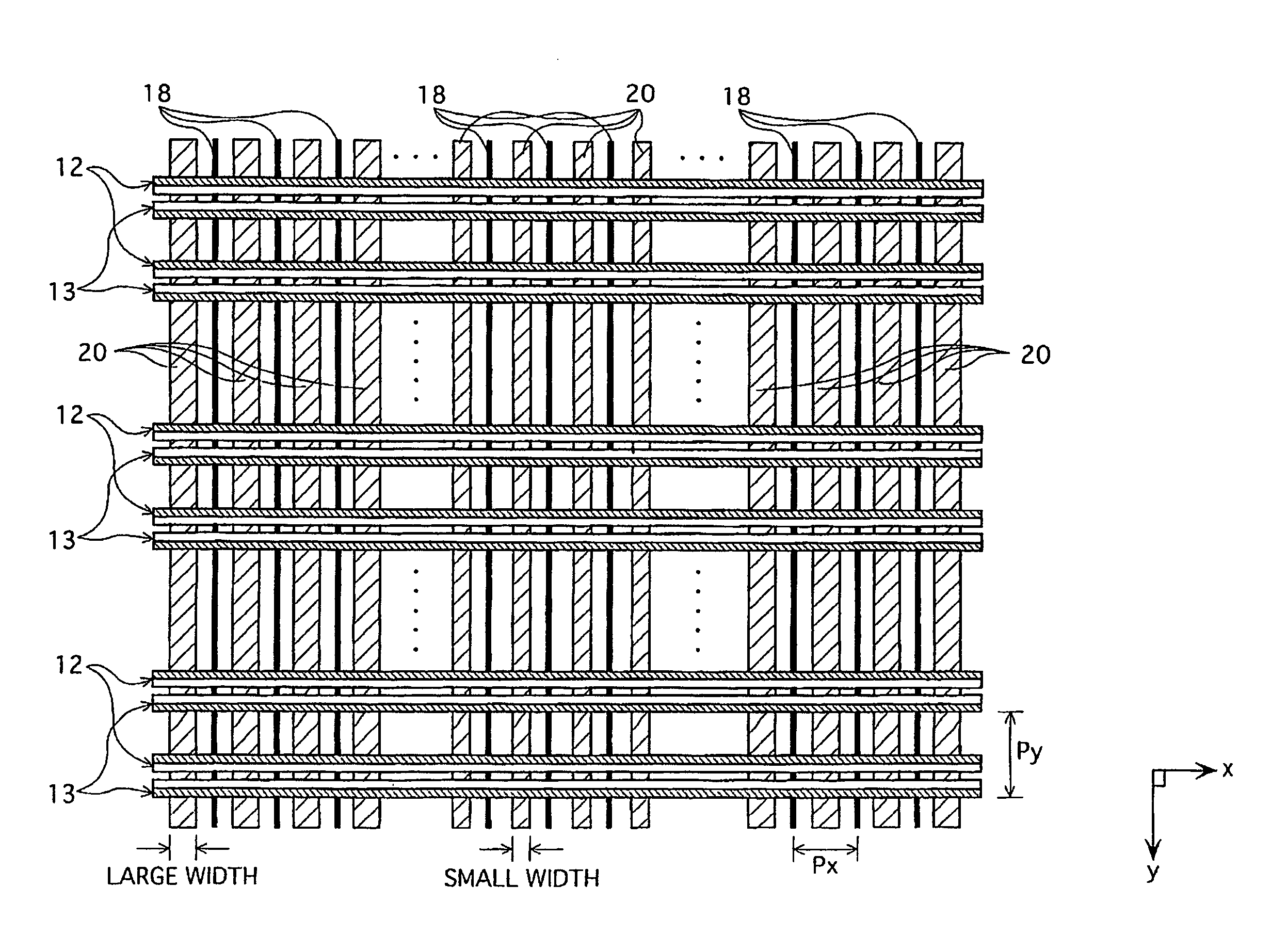
[0109]FIG. 6 shows an arrangement of the display electrodes 12 (X) and 13 (Y) within the display region of the PDP 1. FIG. 7 is a schematic view presenting the arrangement of the display electrodes 12 and 13 within the above display region in more detail.
[0110] As shown in FIG. 7, a second embodiment has the following characteristic. The display electrodes 12 and 13 that are arranged so as to be adjacent to each other in the vertical direction of the panel (the y direction) (strictly speaking, the transparent electrodes 120 and 130) gradually increase in width from the central region of the panel in the y direction towards the top and bottom edges of the panel.
[0111] The dimensions of various parts of the above PDP 1 are, for example, as follows.
[0112] The gap between one display electrode 12 and one display electrode 13 forming one pair: 80 μm to 100 μm
[0113] The width of one transparent electrode: 215 μm to 320 μm
[0...
third embodiment
[0127] Third Embodiment
[0128] [3.1. Construction of the PDP]
[0129]FIG. 10 is a schematic view showing, in detail, the arrangement of the display electrodes 12 and 13 in a third embodiment.
[0130] As shown in FIG. 10, the third embodiment has the following characteristic. The bus lines 121 and 131 gradually increase in width from the central region of the panel in the y direction towards the top and bottom edges of the panel. The bus lines 121 and 131 are included in the display electrodes 12 and 13 that are arranged so as to be adjacent to each other in the vertical direction of the panel (the y direction).
[0131] The dimensions of the various parts of the above PDP 1 are, for example, as follows.
[0132] The gap between one display electrode 12 and one display electrode 13 forming one pair: 90 μm
[0133] The width of the transparent electrode: 100 μm
[0134] The width of the bus line: 40 μm to 100 μm
[0135] The pitch Px: 360 μm
[0136] The pitch Py: 1080 μm
[0137] With this constructio...
PUM
 Abstract
Description
Claims
Application Information
 - Generate Ideas
- Intellectual Property
- Life Sciences
- Materials
- Tech Scout
- Unparalleled Data Quality
- Higher Quality Content
- 60% Fewer Hallucinations
Browse by: Latest US Patents, China's latest patents, Technical Efficacy Thesaurus, Application Domain, Technology Topic, Popular Technical Reports.
© 2025 PatSnap. All rights reserved.Legal|Privacy policy|Modern Slavery Act Transparency Statement|Sitemap|About US| Contact US: help@patsnap.com