Surface-mounted light-emitting diode and method

a surface-mounted light-emitting diode and light-emitting diode technology, which is applied in the direction of semiconductor/solid-state device manufacturing, electrical apparatus, semiconductor devices, etc., can solve the problems of thermal expansion coefficient difference, side through-hole printed circuit board, and added constraints to improve the density of components

Inactive Publication Date: 2005-03-03
STANLEY ELECTRIC CO LTD
View PDF10 Cites 82 Cited by
  • Summary
  • Abstract
  • Description
  • Claims
  • Application Information

AI Technical Summary

Problems solved by technology

The double-sided through-hole printed-circuit board, however, has a thickness of at least 0.1 mm, which is a factor that interferes with the goal of thinning the surface-mounted LED.
An accumulated area of the fillets adds constraints to improving the component density mounted on the mounting board.
A sharp variation in temperature on thermosetting and cooling of the sealing resin for the surface-mounted LED, or on heating and cooling of the solder reflow, may cause a stress between the double-sided through-hole printed-circuit board and the sealing resin, which have a difference in thermal expansion coefficient.
The stress results in quality-related malfunctions such as breaks in the LED chip, wire disconnection, and peel at the interface between the double-sided through-hole printed-circuit board and the sealing resin.
Such burrs inhibit the solder from elevating onto the metallic conductive patterns on the surface-mounted LED, resulting in insufficient soldering between the surface-mounted LED and the mounting board.
Therefore, any improvements are not applied in light extraction efficiency when a semiconductor light-emitting element is mounted, and are not applied in constructions associated with optics to control distribution of light.
Accordingly, a light source has a poor optical characteristic.

Method used


Image

  • Surface-mounted light-emitting diode and method
  • Surface-mounted light-emitting diode and method
  • Surface-mounted light-emitting diode and method

Examples


embodiment

[0053] Embodiment of FIG. 9

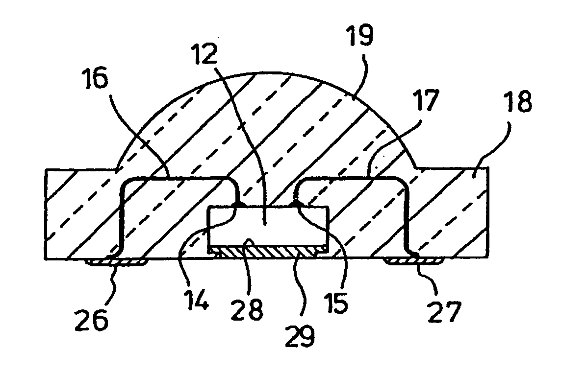
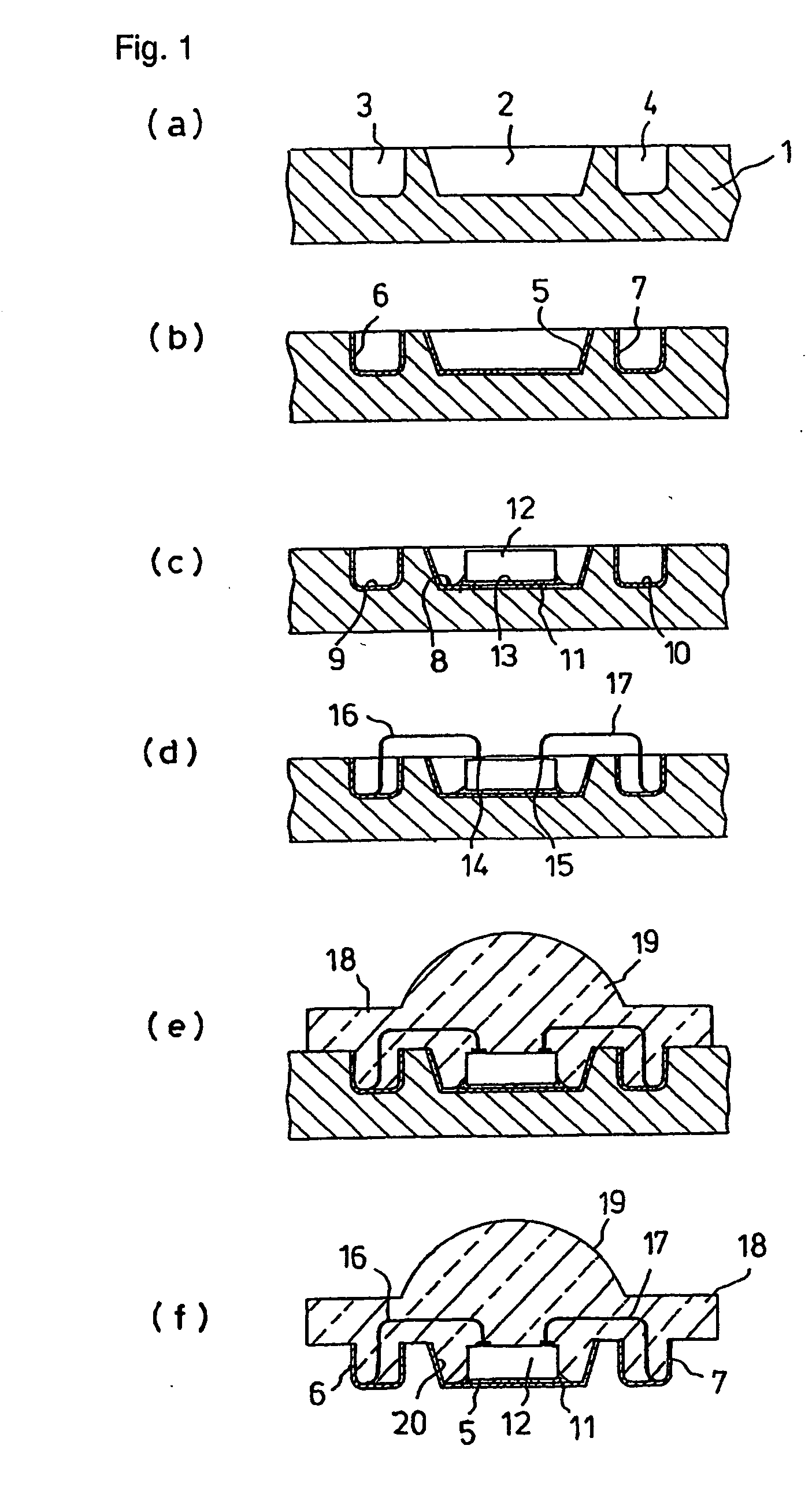
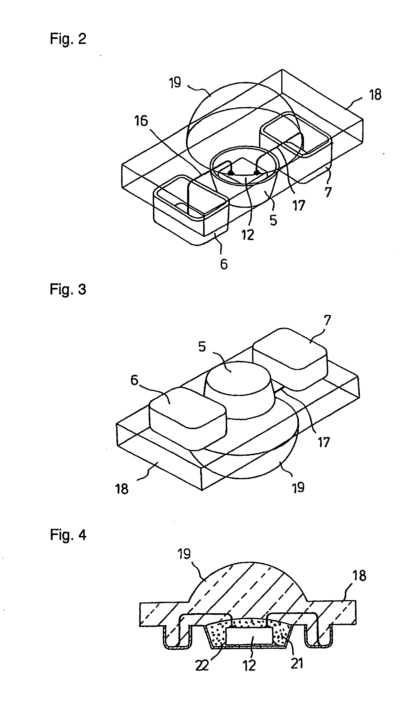
[0054]FIG. 9 is a cross-sectional view showing another embodiment of the invention. In this embodiment, an insulator member 29 can be disposed below the bottom 28 of the LED chip 12. The upper electrodes 14, 15 on the LED chip 12 can be connected to ends of the wires 16, 17. The metallic films 26, 27 can be connected to other ends of the wires 16, 17 to achieve an electric connection between the upper electrodes 14, 15 on the LED chip 12 and the metallic films 26, 27. These metallic films 26, 27 are preferably the only ones that are formed on the surface of the optically transmissive resin 18 in this embodiment. Also in this embodiment, the optically transmissive resin 18 may be formed to include the lens 19 above the LED chip 12 to collect and guide the light emitted from the LED chip 12. Alternatively, the optically transmissive resin 18 may be formed to keep the flat emission surface of the optically transmissive resin 18 to refract the light that reach...


PUM


Abstract

A surface-mounted light-emitting diode can be employed as a light source for cell phones and other electronic devices and contributes to the downsizing of electronic devices. An optically transmissive resin can have a surface provided with metallic films formed thereon and be employed to seal an LED chip and wires therein. The LED chip can be mounted on the metallic film via a conductive adhesive to achieve an electrical connection between a lower electrode of the LED chip and the metallic film. The wires can be connected between upper electrodes of the LED chip and the metallic films to achieve electrical conduction between the upper electrodes of the LED chip and the metallic films.

Description

[0001] This invention claims the benefit of Japanese patent application No. 2003-307517, filed on Aug. 29, 2003, which is hereby incorporated by reference. BACKGROUND OF THE INVENTION [0002] 1. Field of the Invention [0003] The present invention relates to a light-emitting diode and more particularly to a surface-mounted light-emitting diode that contains no printed-circuit board and is available in illumination light sources for compact and lightweight devices such as cell phones and other electronic devices. [0004] 2. Description of the Related Art [0005] With recent efforts to downsize and reduce the weight of electronic devices, different approaches have been aggressively developed for surface mounting aimed at downsizing a light-emitting diode (LED). A conventional structure of a surface-mounted LED includes an insulator substrate that provides both surfaces with a pair of metallic conductor patterns that are electrically connected via a through-hole to form a double-sided thro...

Claims


Application Information

Patent Timeline
Patent Type & Authority Applications(United States)
IPC IPC(8): H01L33/50H01L33/54H01L33/56H01L33/60H01L33/62
CPCH01L21/568H01L2224/32245H01L33/486H01L33/54H01L33/62H01L2224/48465H01L2224/73265H01L2224/85001H01L2924/01078H01L2924/01079H01L2924/12041H01L21/6835H01L2224/48247H01L2224/83001H01L2924/1815H01L2224/92247H01L2924/00H01L2224/48095H01L2224/8592H01L2924/181H01L2924/00012
Inventor ABE, TOMOAKISUWA, HISASHI
Owner STANLEY ELECTRIC CO LTD
Why Eureka
Try Eureka