Film mapping system

a mapping system and film technology, applied in the field of film mapping system, can solve the problems of limiting the performance of this system, requiring mechanical movements of the wheel assembly, and being undesirable for precise measurements

Active Publication Date: 2005-03-03
SVT ASSOCS
View PDF17 Cites 96 Cited by
  • Summary
  • Abstract
  • Description
  • Claims
  • Application Information

AI Technical Summary

Benefits of technology

The present invention is a system that uses electromagnetic radiation to measure the properties of materials. It includes an electromagnetic radiation source and multiple radiation convergence elements. The incident beams of electromagnetic radiation are received by the radiation convergence elements and converted into smaller output beams with perpendicular cross sections. These output beams then intersect with a selected material at the measuring location. The system can measure various properties of the material by analyzing the interactions between the electromagnetic radiation and the material.

Problems solved by technology

The patent text discusses the use of LED-based spectrometers for precise measurements in various fields such as semiconductor and photonics metrology. However, existing LED spectrometers have limitations in wavelength resolution and stability, making it difficult to achieve high-resolution measurements. The technical problem addressed in the patent text is to provide a new technology to overcome these limitations and provide better wavelength selection for precise measurements.

Method used


Image

  • Film mapping system
  • Film mapping system
  • Film mapping system

Examples


Embodiment Construction

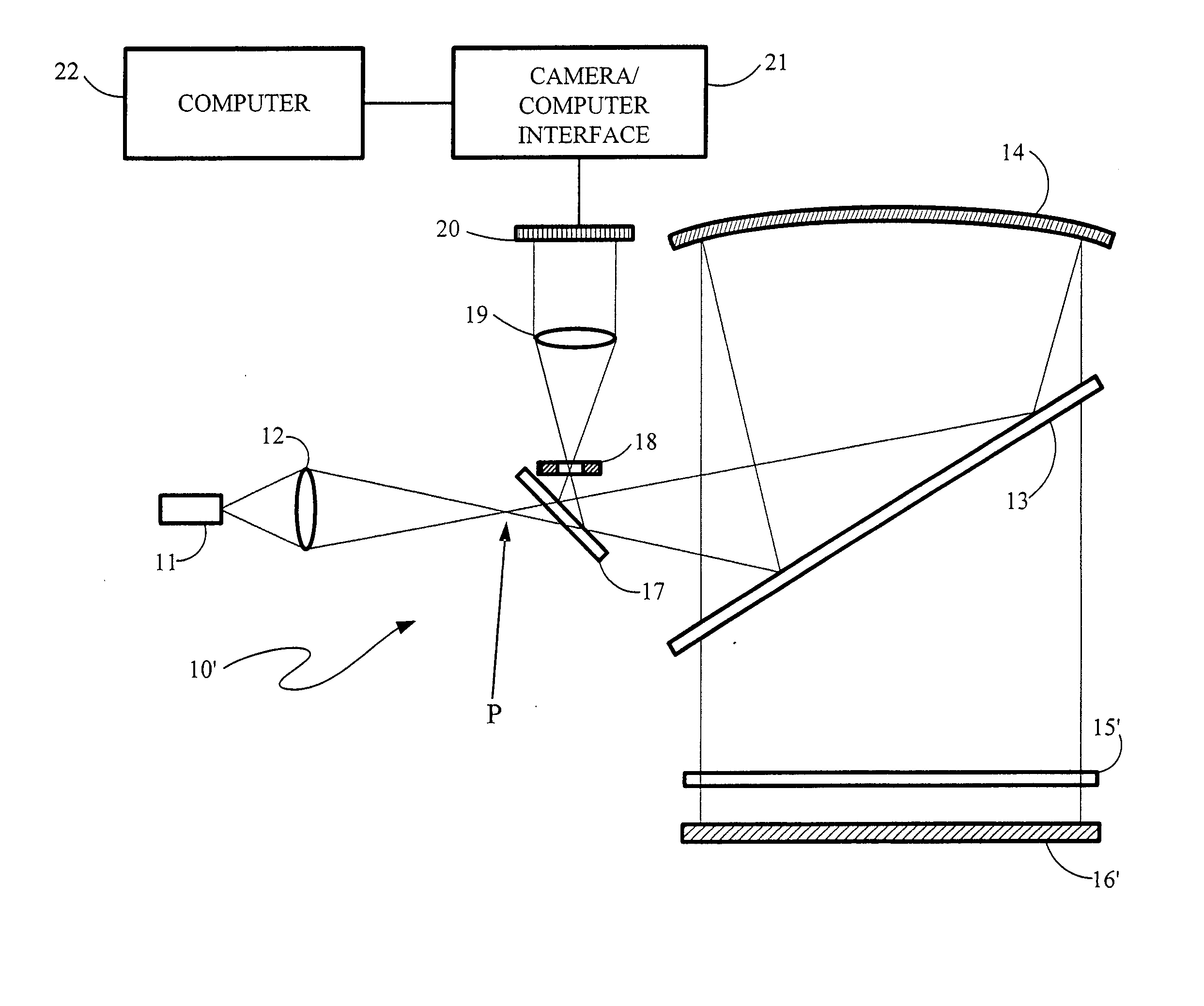
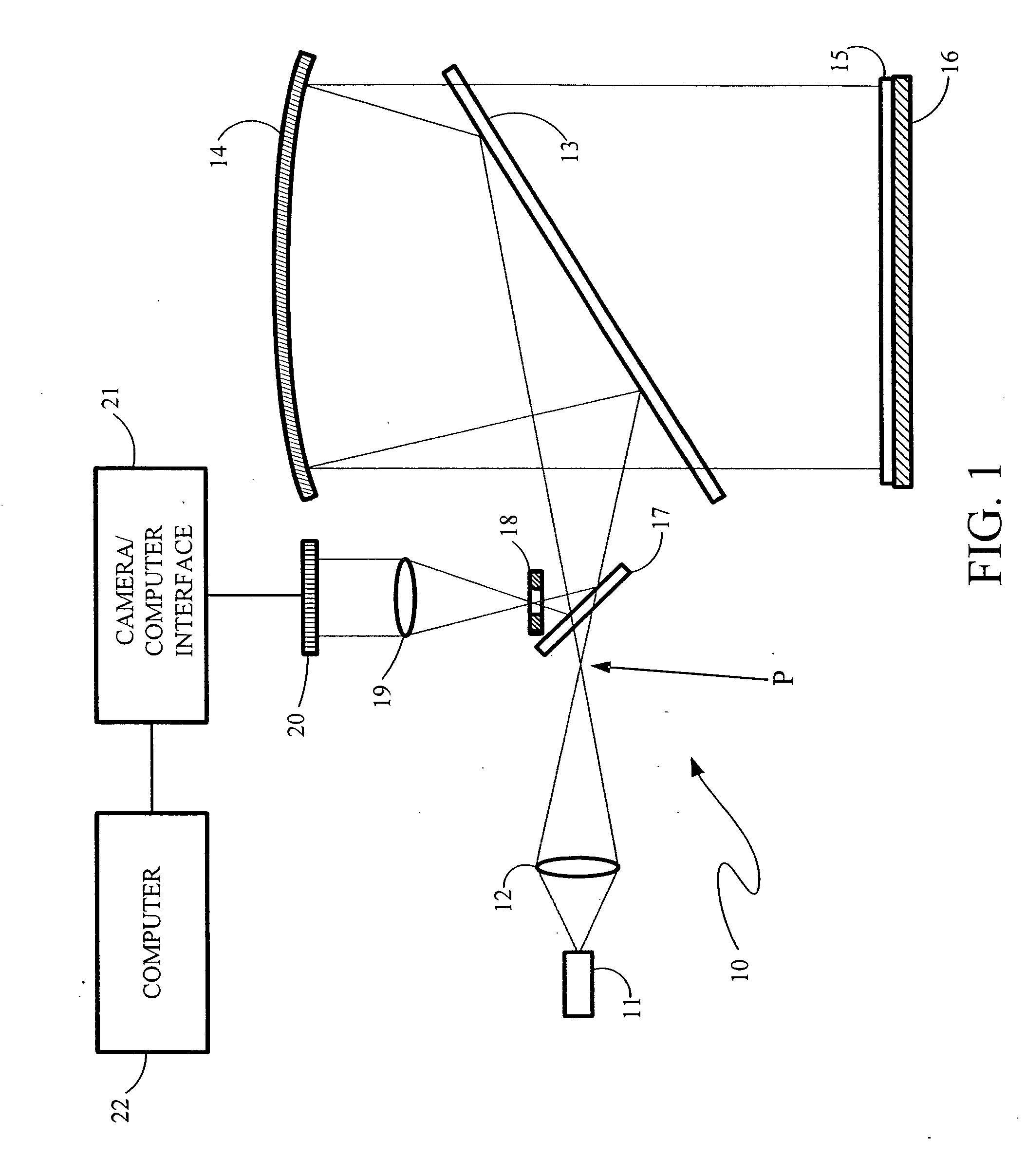
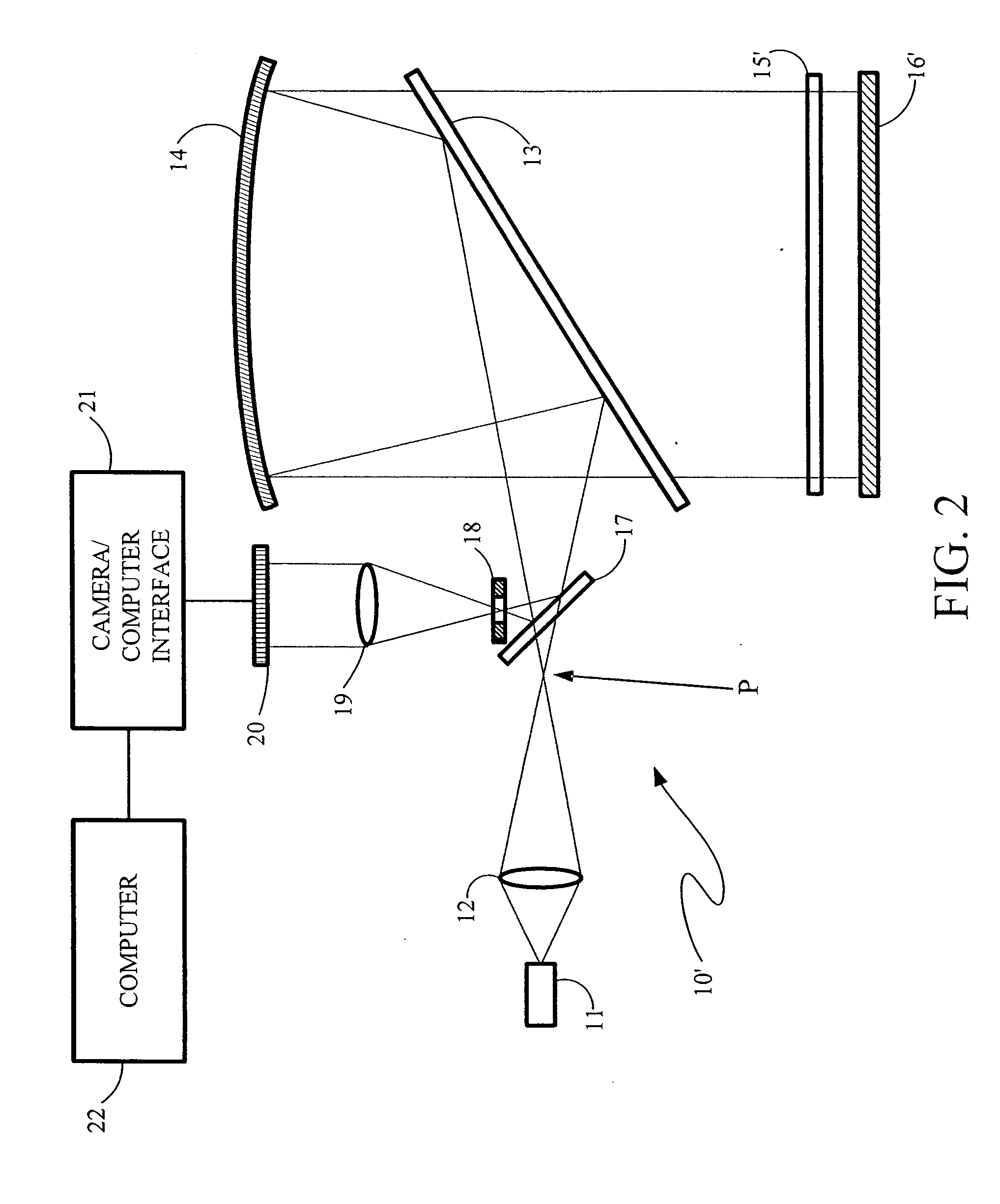
FIG. 1 shows a rapidly operating, complete thin-film specimen measurement system, 10, having a broadband light source, 11, simulating a white light source, and that is formed by an array of narrowband light sources, such as laser diodes or light-emitting diodes. A more detailed description of array 11 of narrowband light sources will be given below. Thin-films of solid materials are used as examples herein but such measurements can also be made of gaseous or liquid materials appropriately provided for such measuring, or combinations thereof.

An illumination lens, 12, near the light source 11, a large aperture beamsplitter, 13, and an on-axis parabolic (or, alternatively, spherical) mirror, 14, together form a large aperture, complete specimen illumination system for directing light emitted by source 11 to illuminate a film specimen, 15, supported on a substrate, 16. A small aperture beamsplitter, 17, is positioned in the illumination light path with the unwanted, but unavoidable, ef...


PUM


Abstract

A materials properties measuring system for using electromagnetic radiation interactions with selected materials positioned at a measuring location to determine selected properties thereof having an electromagnetic radiation source along with a plurality of radiation convergence elements for receiving any incident beams of electromagnetic radiation including the source having corresponding selected cross sections substantially perpendicular to the input path, and for converging these incident beams into corresponding departing beams including to the selected material each having a selected cross section substantially perpendicular to the output path that is smaller than that of its corresponding incident beam, and transmitting them to a beamsplitter that has an area as great as any such element. An electromagnetic radiation receiver is provided to receive any beams of electromagnetic radiation incident thereon after propagating thereto from the beamsplitter. The electromagnetic radiation source for providing propagating selected electromagnetic radiation at an output thereof is formed by a plurality of electromagnetic radiation emitters with differing center emission wavelengths and a beam combiner is provided with them wherein any electromagnetic radiation emitted by any of said electromagnetic radiation emitters enters at differing points to follow at least in part a common optical path to an output through at least some portion of the combiner determined by reflections and transmissions thereof in and at the combiner.

Description


Claims


Application Information

Patent Timeline
Owner SVT ASSOCS
Why Eureka
Try Eureka