Semiconductor device and manufacturing method of semiconductor device

a semiconductor device and semiconductor technology, applied in the field of semiconductor devices, to achieve the effect of simple configuration, stable connection, and thinning of semiconductor devices

Active Publication Date: 2005-03-10
LAPIS SEMICON CO LTD
View PDF5 Cites 0 Cited by
  • Summary
  • Abstract
  • Description
  • Claims
  • Application Information

AI Technical Summary

Benefits of technology

[0026] According to the semiconductor device according to the second present invention, since a portion of the side surface of the semiconductor chip is covered with the support member to fix the semiconductor chip from the side surface, it is possible to make the support member thinner.
[0027] According to the manufacturing method of the semiconductor device of the present invention, there is an advantage to form a support member for fixing the semiconductor chip between the leads without giving the stress on the leads.
[0028] In addition, according to the semiconductor device of the first present invention, there is an advantage to provide the stable connection between the semiconductor chip and the leads.
[0029] In addition, according to the semiconductor device of the second present invention, there is an advantage to make the semiconductor device thinner with the simple configuration.

Problems solved by technology

However, the above-described semiconductor device involves a problem such that, in the event of using the large island, due to heat applied upon mounting the island on the device, a difference of a coefficient of thermal expansion between metal to be used for the island and the sealing resin is generated, so that the island is stripped off from the sealing resin and the island cracks at a lower surface of the semiconductor device.
However, according to the above-described suggestion, since the resin film is thermo-compressed on the inner leads and the resin film is implanted between the inner leads, this involves a problem such that a stress is applied to the inner lead upon the thermo compression so that the lead is modified.

Method used


Image

  • Semiconductor device and manufacturing method of semiconductor device
  • Semiconductor device and manufacturing method of semiconductor device
  • Semiconductor device and manufacturing method of semiconductor device

Examples


first embodiment

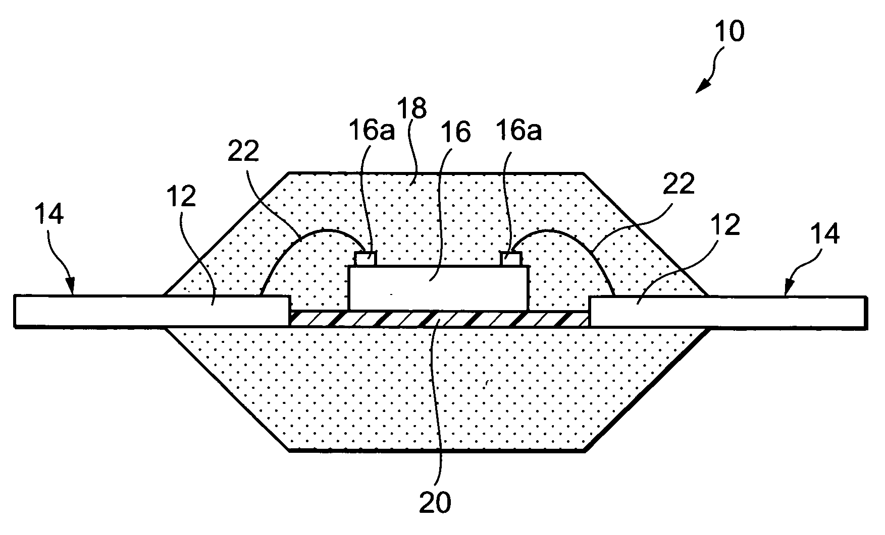
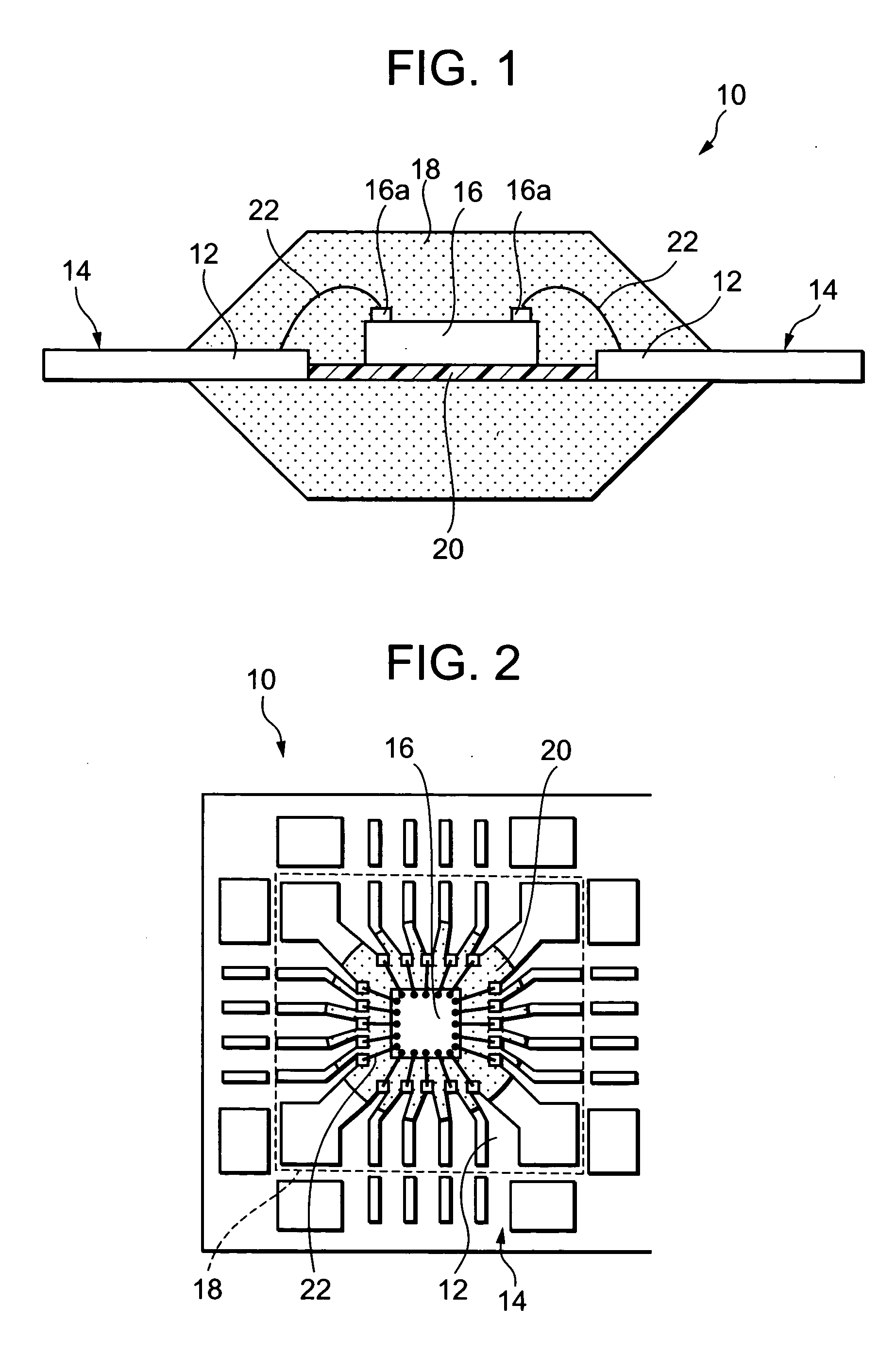
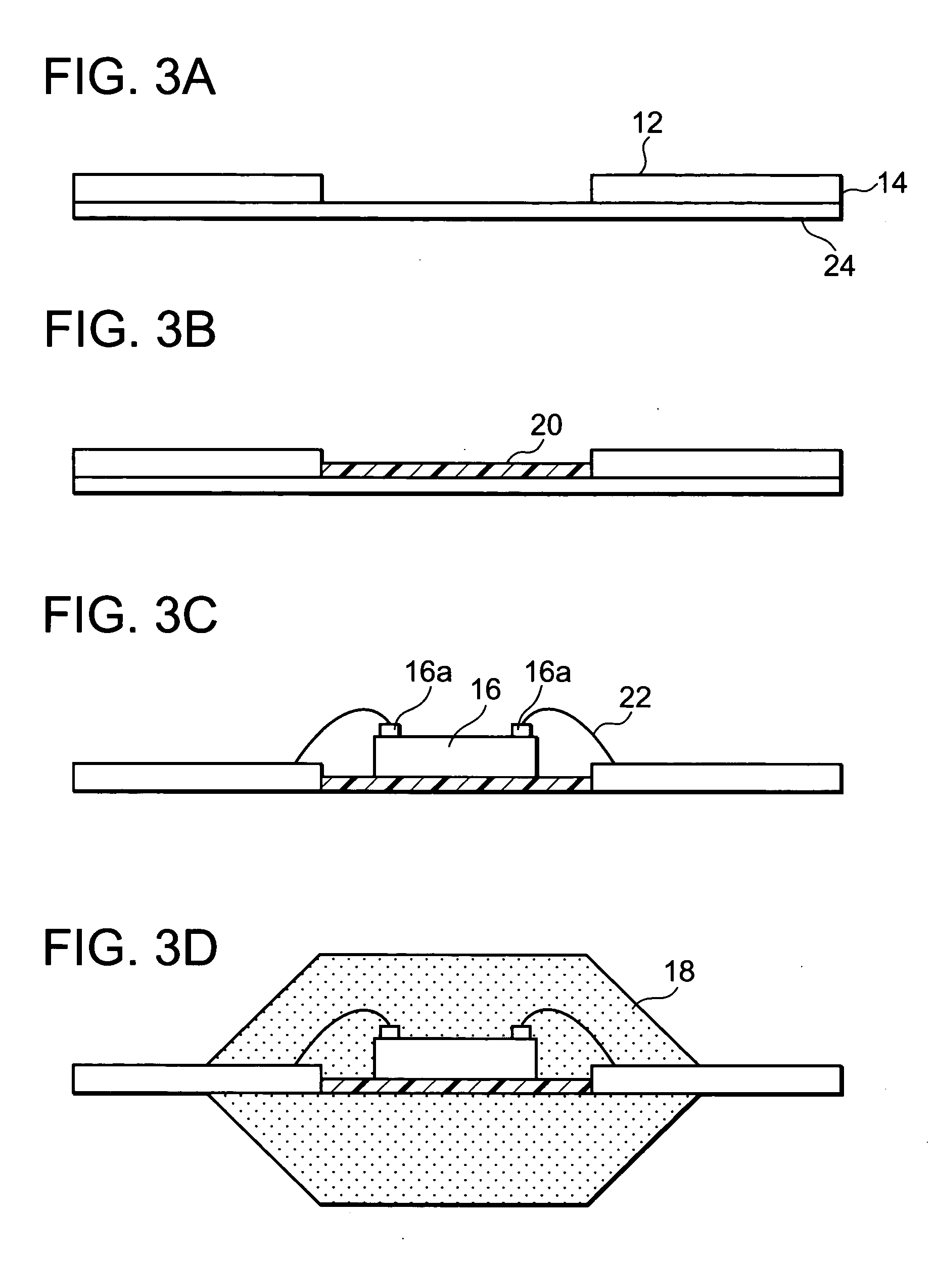
[0040]FIG. 1 is a schematic sectional view showing a semiconductor device according to a first embodiment of the present invention, FIG. 2 is a plan view showing the semiconductor device according to the first embodiment of the present invention, and FIG. 3 is a step view showing a manufacturing method of the semiconductor device according to the first embodiment of the present invention.

[0041] A semiconductor device 10 may include a plurality of leads 12 composing a lead frame 14 and a semiconductor chip 16, which are sealed by sealing resin 18.

[0042] The plural leads 12 are arranged so as to surround the semiconductor chip 16. In addition, in the region surrounded by the front ends of the leads 12 (the region where the semiconductor chip 16 is arranged) and between the front ends of the adjacent leads 12, an insulative island made of resin (an insulative support member) is formed with implanted therein, and at the side surface of the front ends of the leads 12, the resin island ...

second embodiment

[0053]FIG. 5 is a schematic sectional view showing a semiconductor device according to a second embodiment of the present invention, and FIG. 6 is a step view showing a manufacturing method of the semiconductor device according to the second embodiment of the present invention.

[0054] According to the present embodiment, the front end 12a of the lead 12 (the connection portion: the bonded surface) projects rather in a thickness direction as compared to the other portions of the lead 12, namely, the connection portion 12a of the lead 12 is thicker than the other portions thereof. Further, this front end 12a is electrically connected to the bonding pad 16a of the semiconductor chip 16 by the bonding wire 22. The explanation except for this point will be herein omitted because the present embodiment is identical with the above-described first embodiment other than this point.

[0055] Hereinafter, a manufacturing method of the semiconductor device 10 according to the present embodiment w...

third embodiment

[0063]FIG. 7 is a schematic sectional view showing a semiconductor device according to a third embodiment of the present invention, and FIG. 8 is a step view showing a manufacturing method of the semiconductor device according to the third embodiment of the present invention.

[0064] According to the present embodiment, the semiconductor chip 16 (the side surface of the semiconductor chip 16) is partially implanted in the resin island 20 so that the semiconductor chip 16 is supported and fixed by the resin island 20. In other words, the side surface of the semiconductor chip 16 is partially covered with the resin island 20. The explanation except for this point will be herein omitted because the present embodiment is identical with the above-described first embodiment other than this point.

[0065] Hereinafter, the manufacturing method of the semiconductor device 10 according to the present embodiment will be described below.

[0066] At first, the mold member 24 shaped in a tape or a m...


PUM


Abstract

To provide a manufacturing method of a semiconductor device, in which a support member for fixing a semiconductor chip is formed between leads without giving stress to the leads. The semiconductor device may comprise a plurality of leads composing a lead frame, a resin island (a support member) that is formed between the leads, and a semiconductor chip that is fixed on the resin island and is electrically connected to the leads by bonding wires, and sealing resin for partially sealing the semiconductor chip, the bonding wire, and the lead by resin, wherein a liquid cured resin is formed (filled) between the leads to form the resin island (the support member).

Description

BACKGROUND OF THE INVENTION [0001] 1. Field of the Invention [0002] The present invention relates to a semiconductor device of a resin seal type using a lead frame, and a manufacturing method of the same. [0003] This application is counterpart of Japanese patent application, Serial Number 317109 / 2003, filed Sep. 9, 2003, the subject matter of which is incorporated herein by reference. [0004] 2. Description of the Related Art [0005] Conventionally, in a semiconductor device of a resin seal type, a semiconductor chip is mounted on a lead frame to be sealed by resin. The lead frame is made of metal, and has an island together with leads. The semiconductor chip is loaded and fixed on the island, and at the same time, a bonding pad and the leads, which are formed on a semiconductor chip, are electrically connected with each other. [0006] However, the above-described semiconductor device involves a problem such that, in the event of using the large island, due to heat applied upon mountin...

Claims


Application Information

Patent Timeline
Patent Type & Authority Applications(United States)
IPC IPC(8): H01L23/495H01L23/50
CPCH01L23/49506H01L2224/48091H01L2224/48247H01L2224/49171H01L24/49H01L24/48H01L2924/00014H01L2924/00H01L2924/181H01L2224/05554H01L2924/10162H01L2924/00012H01L2224/45099H01L2224/45015H01L2924/207
Inventor INO, YOSHIHIKOKAWANO, HIROSHI
Owner LAPIS SEMICON CO LTD
Why Eureka
Try Eureka