Plasma display device

a technology of plasma display and display device, which is applied in the direction of connection contact material, television system, instruments, etc., can solve the problems of deteriorating production efficiency and increasing production cost and achieve the effect of maximizing the spatial use of plasma display devi

Inactive Publication Date: 2005-03-31
SAMSUNG SDI CO LTD
View PDF7 Cites 26 Cited by
  • Summary
  • Abstract
  • Description
  • Claims
  • Application Information

AI Technical Summary

Benefits of technology

[0023] In addition, in the above embodiments of the present invention, the ground electrode

Problems solved by technology

According to a plasma display device of the prior art, production efficiency of a plasma display device may be deteriorated and prod

Method used


Image

  • Plasma display device
  • Plasma display device
  • Plasma display device

Examples


Embodiment Construction

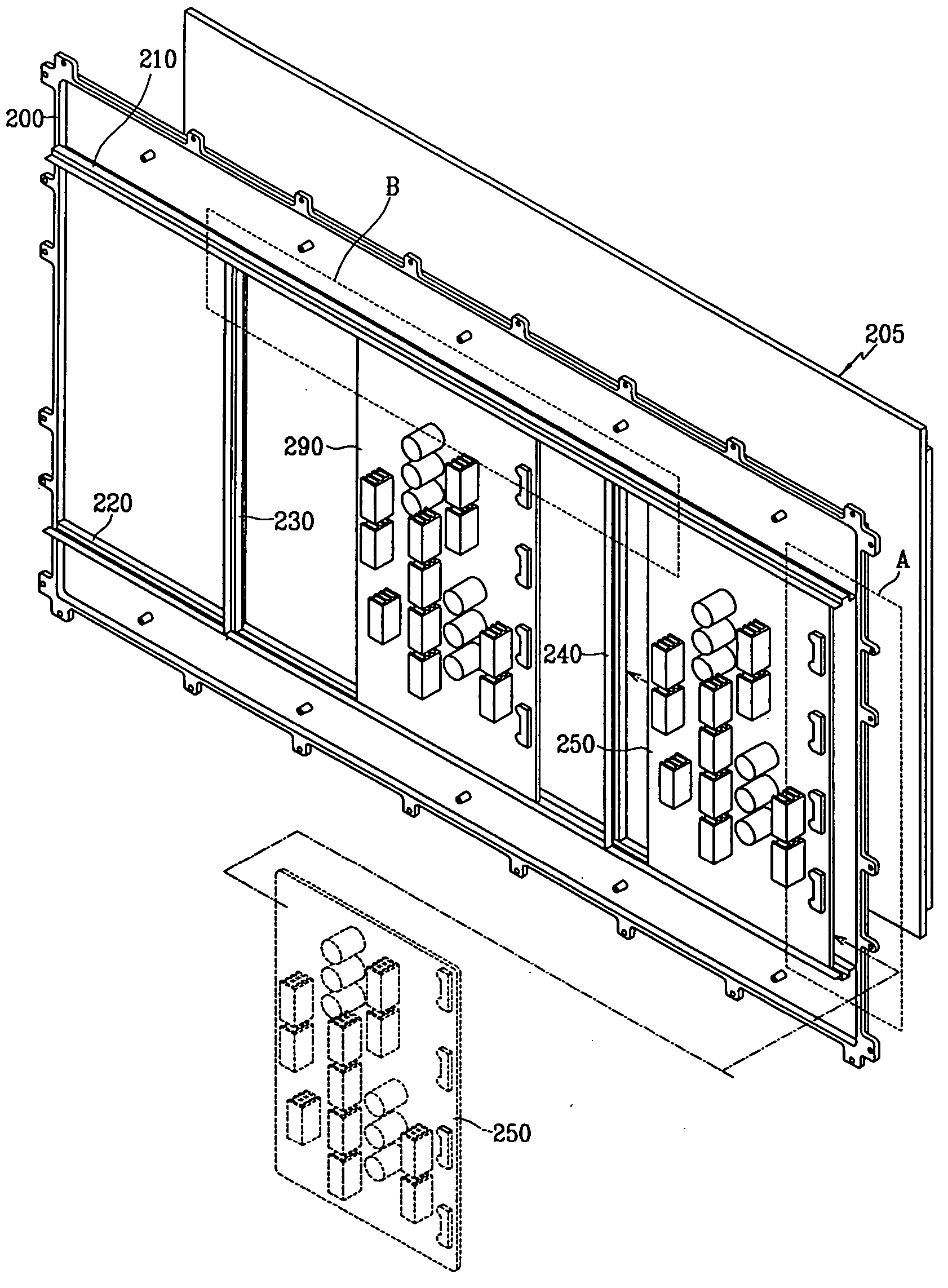
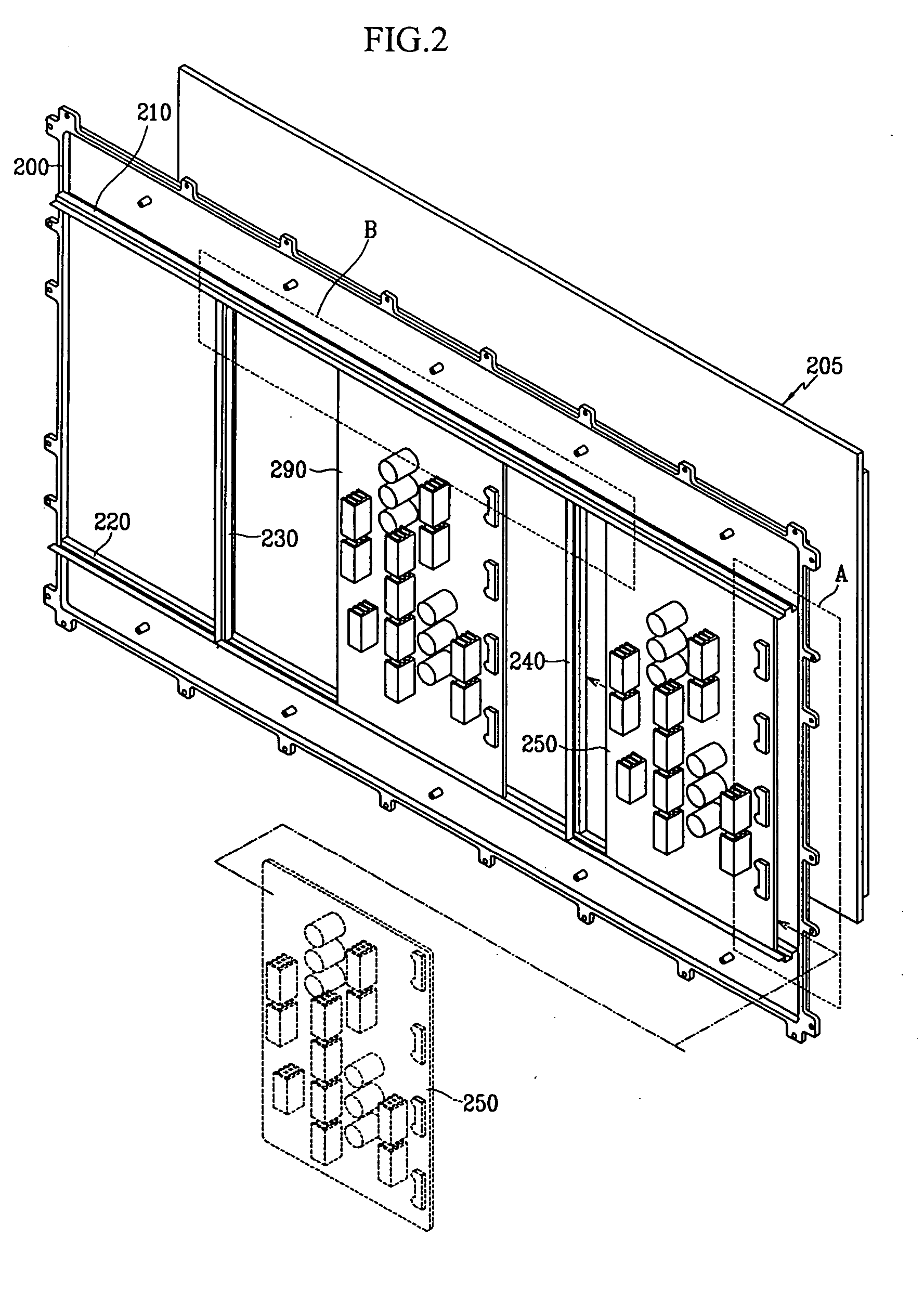
[0031] Referring to FIG. 2, a PDP according to an embodiment of the present invention includes PDP 205, chassis base 200 for supporting PDP 205, a plurality of mounting members 210, 220, 230, 240 mounted on a side of chassis base 200, and at least one PCB 250, 290 mounted to chassis base 200 via the plurality of mounting members 210, 220, 230, 240.

[0032]FIG. 2 illustrates first, second, third, and fourth mounting members 210, 220, 230, 240 as an example of the plurality of mounting members. However, the present invention should not be understood as limited to a specific number of mounting members.

[0033] At least one mounting member of the plurality of mounting members 210, 220, 230, 240 has a guide groove for guiding at least one PCB 250, 290. As shown in FIG. 3, first and second guide grooves 310, 320 are formed at first and second mounting members 210, 220 according to the present embodiment.

[0034] The method of attaching mounting members 210, 220, 230, 240 are mounted to chass...


PUM


Abstract

At least one mounting member having a guide groove mounted on a side of a chassis base for supporting a plasma display panel, and at least one printed circuit board slidingly mounted along the guide groove. Such mounting of a printed circuit board enables enhancement of production efficiency. By forming a ground electrode on the PCB along a position contacting the guide groove, grounding of the PCB is enhanced and electromagnetic interference thereof is minimized.

Description

CROSS REFERENCE TO RELATED APPLICATIONS [0001] This application claims priority to and the benefit of Korean Patent Application No. 2003-55829 filed on Aug. 12, 2003 in the Korean Intellectual Property Office, the entire content of which is incorporated herein by reference. FIELD OF THE INVENTION [0002] Generally, the present invention relates to a plasma display device. More particularly, the present invention relates to a plasma display device having an enhanced mounting structure of a printed circuit board to a chassis base. BACKGROUND OF THE INVENTION [0003] As is well known in the art, a plasma display device realizes a desired image using plasma discharge. Such a plasma display device generally includes a plasma display panel (PDP) for realizing the desired image through plasma discharge, which is activated by an external power source; a chassis base for firmly holding the PDP and for forming structural strength of a plasma display device; a driving circuit for driving the PDP...

Claims


Application Information

Patent Timeline
IPC IPC(8): H01J17/49G09G3/28H01R4/64H05K7/14H05K9/00
CPCG09G3/28H05K9/0039H05K7/1418H01R4/64H04N5/645H01J17/16H01J11/10
Inventor OH, SE-IL
Owner SAMSUNG SDI CO LTD
Why Eureka
Try Eureka